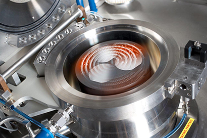
Through a recent NSF MRI award (DMR-1337592) RIT has purchased and installed a metal organic vapor phase epitaxy (MOVPE) system for growth of III-V thin film crystals and nanostructures. The equipment, shown in figure below, consists of an Aixton 3×2” Close Coupled Showerhead (CCS) metalorganic vapor phase epitaxy (MOVPE) system. This system is targeted specifically to R&D customers and offers outstanding growth uniformity, temperature control, and high source utilization efficiency. This system has also been proven to provide excellent thickness, composition, and doping control over a very wide parameter space, as well as the flexibility in growth conditions necessary for various types of materials and nanostructures. The gas circuit for the MOVPE allows for an exceptionally large range of III-V nanomaterials to be grown, depending on what sources and gas are actually used. Initial source materials will include As, P, Sb, In, Ga and Al as well as Zn, Si and C dopants. In-situ diagnostic capability are provided by a EpiTTCurve optical pyrometer system for real-time in-situ monitoring of temperature, strain and reflectivity. The EpiTTCurve will allow rapid prototyping of structures and extreme precision and repeatability of temperature and lattice constants.
MOVPE is available to both internal and external customers. Click here for information on MOVPE rates and how to obtain a quote.


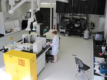
This facility houses a variety of ultra-high vacuum and thin film deposition systems including three Lesker PVD75 evaporators (both thermal and sputtering).
The capabilities of The Semiconductor & Microsystems Fabrication Laboratory (SMFL) include:
- Photovoltaics and Optoelectronics Characterization
- Ocean Optics HR4000 Spectrometer (vis-NIR) and NIR512 Spectrometer (NIR)
- ASD Feildspec spectroradiometer for calibrated spectral irradiance
- Cooke Sensicam QE electroluminescence camera and mount
- Bio-Rad 575C Enhanced Intensity FTIR Spectroscopic Microscope
- Coherent 300mW Ar-ion laser
- General Materials Characterization
- Accent HL5550 Hall System with Cryogenic Stage
- PE Lamda 900 UV-Vis-NIR
- TA Instruments Q-series DSC and TGA
- Quantachrome Nova 1000e BET
- TA Instruments DMA
- Microscopy
- Nikon Eclipse Digital Nomarski Microscope
- Zeiss Digital Microscopic Imaging System
- Hitachi S-900 High Resolution Near Field FE-SEM
- Multi-wavelength Jobin Yvon Horriba Raman Microscope
- KLA Tencor HRP75 High Resolution Profiler
- Thin Film Deposition
- Lesker PVD75 Thermal Evaporator
- Lesker PVD75 Torus Sputtering System
- Lesker Nano38 Thermal Evaporator
- Gold Electroplating System
For a complete list of available tools go to https://wiki.rit.edu/display/smfl/Tool+Set
In this facility photovoltaic solar cells are tested under simulated sunlight conditions. The Oriel AM1.5 and AM0 solar simulator, Agilent B1500 Semiconductor Parametric Analyzer and the Optronics Labs OL-750S Spectroradiometer provide the light IV and spectral response tools for our solar cell. Additional characterization of nanomaterials electronic properties can be performed using the spectroradiometer, probe stations and IR cameras.
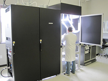
TS Space Systems two-zone close match solar simulator:
The solar simulator is a dual source 18 kW system, custom built by TS Space Systems. The ultraviolet and visible (UV-VIS) portion of the spectrum are created using a 6 kW mercury halide arc lamp (also known as a hydrargyrum medium-arc iodide lamp, or HMI), while infrared (IR) was produced from a 12 kW quartz tungsten halogen (QTH) lamp. The output from these lamps was individually filtered to produce either AM0 or, with the insertion of an additional filter set, AM1.5G. The beams of the two luminaries then combine through a dichroic mirror which reflects below, and transmits above, 750 nm. The combined beams leave the tool parallel to the floor, and were folded onto the test plane by a protected silver front surface mirror. The test plane was composed of a water cooled brass chuck, 330 mm in diameter, which holds cells in place with integrated vacuum lines. The cooled chuck has a temperature range of roughly 10°C to 90°C. The system was designed to produce a 300mm diameter beam.
Spectral Response Detection:
Spectral response (SR) measurements can be taken under multiple conditions. An Optronix Labratories OL-750 spectroradiometeric measurement system uses low noise high precision amplification and light power supplies to provide SR measurements with low noise and high dynamic range below 10‑6 A/W. The illumination can be projecting into a Janis variable temperature micro-probe station with the ability of ranging from 4-500K to measure response as a function of temperature. Additional capabilities are provided with the Newport IQE-200 Automated EQE/IQE measurement system. The illumination source can be focused to a 1mm x 2mm spot, which enables relatively high resolution spatial mapping of the spectral response from the sample when coupled with the motorized x/y stage. The system is setup with multiple detectors to measure the reference and reflected light intensity along with the current generated in the sample. This enables the measurement of both external and internal quantum efficiency through the in-situ measurement of reflection from the surface.
Sula Technologies Deep Level Transient Spectroscopy:
Dr. Hubbard’s research group utilizes a state of the art deep level transient spectroscopy (DLTS) system that is used in conjunction with a Cryo Industries closed loop helium cryostat to probe trap states within semiconductors. Virtually all trap parameters can be determined, including density, thermal cross section, energy level and spatial profile. High sensitivity allows for detection of bulk trap densities on the order of 109 atoms/cm3. The cryostat allows temperature ranges from 10-400K, with the possibility of rapid scans up to 100K in 8 minutes. This powerful technique provides the ability to characterize the crystalline quality and defect density of the epitaxial growths that will be enabled by MOVPE.
Electrical and Optical Measurement Setup:
Multiple spectroscopic and electrical test setups are used to characterize the material band structure, diode characteristics and other device metrics. For optoelectronic measurements, a photoluminescence setup is utilized. Samples can be loaded onto a chuck at room temperature, or into the Cryo Industries closed loop He cryostat. The excitation is provided by a Spectra Physics G41 Ar-ion laser that emits at 514.5nm, from which the excitation is focused on the slit of a 0.32 m JY Horiba iHR320 monochromator. Multiple detectors can be mounted to the monochromator, while the Electro-Optical Systems Ge, InGaAs and InAs detectors provide a spectral range from 0.8 to 3.4 µm. The setup is also used for electroluminescence with the addition of an external bias. With a DC light source and a modification to the optics, photoreflectance measurements can also be taken. Both dark current and JSC/VOC measurements can be taken in an enclosed dark probe station. Multiple halogen lamps are powered by a power supply to increase concentration up to four suns while measuring JSC/VOC. Software is programed in LabView to allow a Kiethley 2400 SMU to be used to measure both the dark I-V and JSC/VOC while also extracting seriesand shunt resistances, idealities and dark saturation currents. Additional probing capabilities are provided by a Cascade Microtech Manual Probing Station, which can be used to measure I-V and C-V with an Agilent B1500 Semiconductor Parametric Analyzer