The RIT III-V EPICenter


The RIT III-V EPICenter
A facility for epitaxial growth of III-V materials
About
The RIT III-V EPICenter is a III-V materials growth facility capable of providing small-batch epitaxial services. Since its beginnings in the 1970s, growth of thin films of epitaxial crystals has proven to be extremely successful in manipulation of the fundamental optical, electrical and magnetic properties of materials. The various epitaxial techniques developed over the last 40 years have led to spectacular technological advancements including the lasers and photo-detectors that power the backbone of the internet, many of the transistors used to send and receive signals in our mobile communication devices, high luminous efficiency white lighting (2014 Nobel Prize) and the high efficiency solar cells used to power our satellite network. The area of epitaxy continues to be ripe for scientific discovery and advancement, particularly in terms of nanostructured or novel materials, for use in areas such as new solar cells, integrated photonics and high power electronics, as well as fundamental and applied device physics.
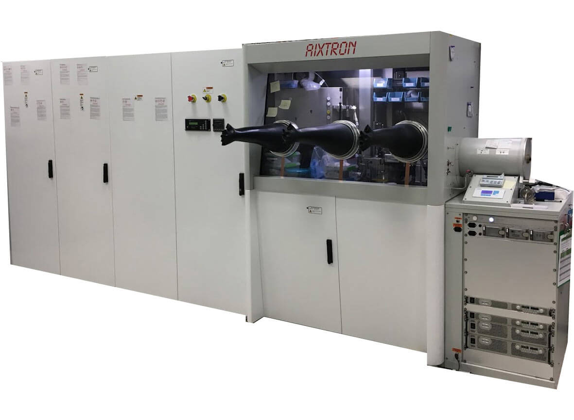
Our researchers have over 30 years of R&D experience with compound semiconductor epitaxial crystal growth, as well as optical and electronic device design and characterization. With research-scale versions of commercial equipment, including an Aixtron Close Coupled Showerhead (CCS) MOCVD, for growing, processing, and/or characterizing compound semiconductor materials and devices, we can provide low-cost, rapid epitaxial services to fit any business.
The center offers a wide range of services, including:
- Low-cost, rapid prototyping of small scale compound semiconductor materials and devices for researchers, companies, and universities.
- III-V fabrication and characterization through the RIT Semiconductor Microsystems Fabrication Lab and the NanoPower Research Laboratories.
- A direct payment model for growth, fabrication, or characterization of compound semiconductor materials and devices.
- Staff support to work with customers for any standard or customized growth or device structure.
See a virtual tour of RIT Semiconductor and Microsystems Fabrication Laboratory
MOCVD Growth
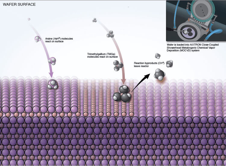
Metalorganic chemical vapor deposition (MOCVD), also called metalorganic vapor phase epitaxy (MOVPE) or organometallic vapor phase epitaxy (OMVPE), is a precisely controllable high quality crystal growth process used in the production of semiconductor electronic, optoelectronic, and photonic devices. Source materials containing a metal atom with organic ligands such as trimethylgallium, and hydrides such as arsine, are injected into a reaction chamber containing crystalline substrate wafers at low pressure and high temperature. The elevated temperature decomposes these precursors into their constituent elements, and the group III and V elements diffuse to the wafer surface where they form chemical bonds which continue the structure templated by the substrate. Through the introduction of varying precursor materials and dopants, a wide range of materials and device structures can be produced.


Growth Capability
We offer several precursor source and material options, in addition to being able to fulfill requests for custom materials. See our current list below or contact us to learn more.
13 precursor sources currently available
| Group-III | Group-V | Dopants |
|---|---|---|
| TMAI, TTBAI | ASH3, TBAs | Si2H6 |
| TMGa, TEGa | PH3 | DETe |
| TMIn | TMSb | DEZn |
| CCI4 |
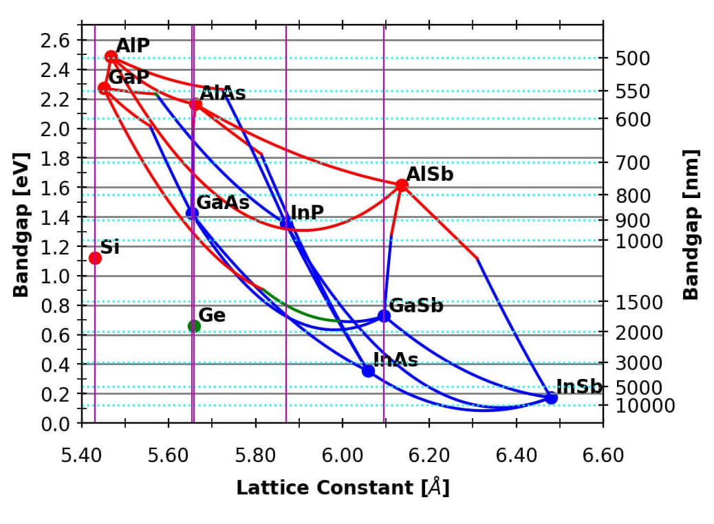
Binary, tertiary, and quaternary materials with variable doping levels
| Binary | Tertiary | Quaternary |
|---|---|---|
| GaAs, InP, GaSb, AlSb, InAs, AlAs, GaP | InGaP, AlInP, InGaAs, InAlAs, GaAsP, AlGaSb | AlGaInP, InGaAsP |
Development of custom materials available upon request.
In addition, susceptors are available for 3 x 2” and 1 x 4” wafers, or pieces of wafers, and GaAs, InP, and GaSb substrates are typically in stock with a variety of doping types and offcuts/orientations. Customers may also supply their own substrates.
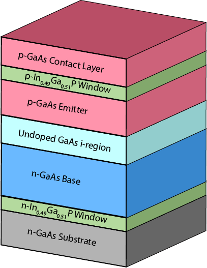
Devices
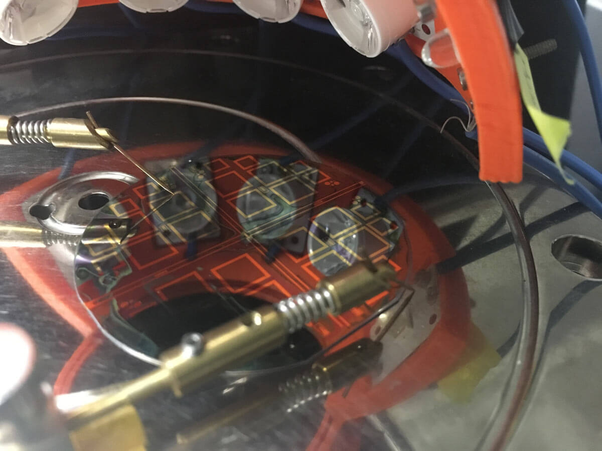
MOCVD can produce a variety of devices and structures including: photovoltaics (PV), light emitting diodes (LED), distributed Bragg reflectors (DBR), laser diodes, vertical cavity surface emitting lasers (VCSEL), transistors, optical detectors, and photomodulators, to name a few.
In addition, the RIT III-V EPICenter team has experience developing quantum well (QW) and quantum dot (QD) structures across a wide range of material systems.
Device wafers can either be shipped directly to the customer or fabricated in-house by our technicians in the RIT SMFL. We also offer various electrical and optical testing capabilities though the NanoPower Research Laboratories.
Metrology Capability
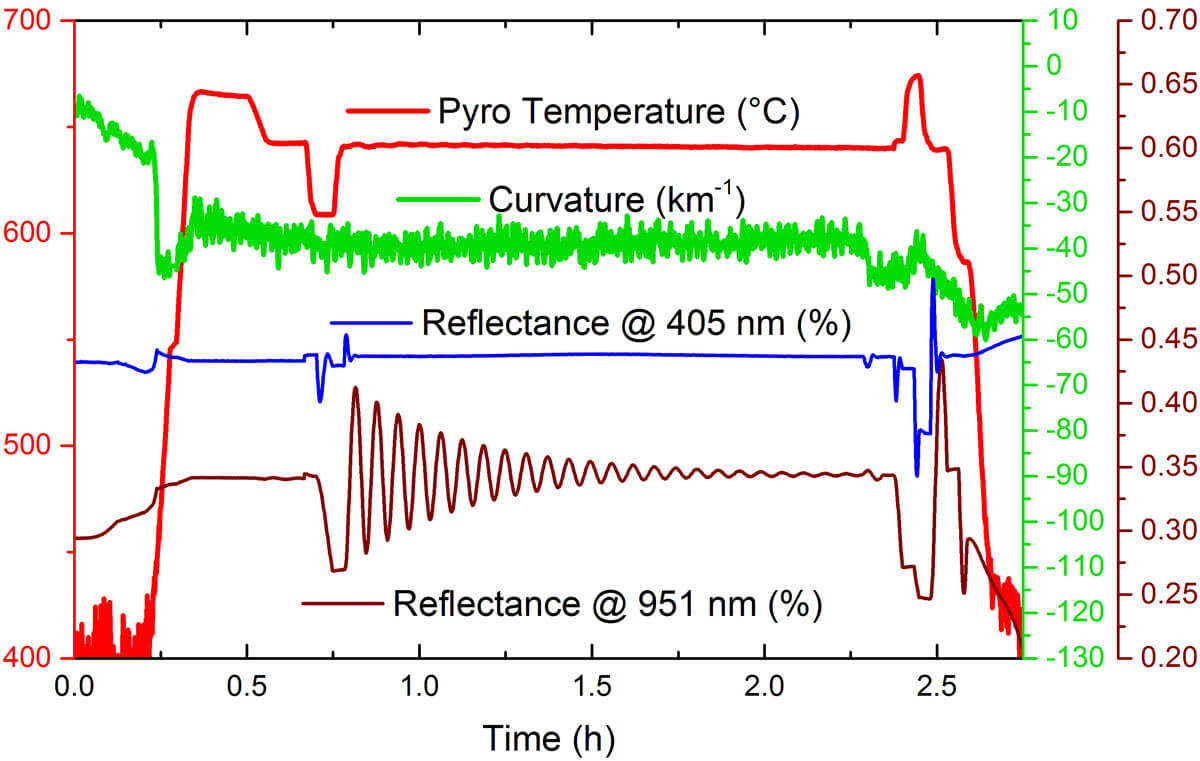
In situ system gives real time feedback of material surface quality from reflectivity at 405 nm, 632 nm, and 951 nm, surface temperature through emissivity corrected pyrometry, and strain through substrate curvature.
Integrated LayTec software analyzes these data to fit against Fabry-Pérot oscillations and extracts the refractive index and extinction coefficients at the measured wavelengths, as well as calculate a precise growth rate and layer thickness.

Nikon Eclipse optical microscope with a differential interference contrast Nomarski prism offers immediate feedback on growth surface morphology. This can offer an initial confirmation of high quality crystal quality. When developing a new material system, coupled to extracted LayTec wafer curvature, 405 nm surface reflectivity, and HRXRD, the source of defect formation or the onset of surface features can be assessed and corrected.

Radiative recombination in direct bandgap materials is an indicator of both material composition and of material quality. A Horiba iHR320 spectrometer with MicOS PL mapping tool and 523 nm diode pumped solid state (DPSS) laser is used with LN2 cooled Si CCD and InGaAs liner array detectors. This allows rapid PL from deepUV to 1.7 µm and wafer mapping across 50- 100mm wafers, and uniformity comparison of peak wavelength, peak intensity, and peak full-width at half-max.
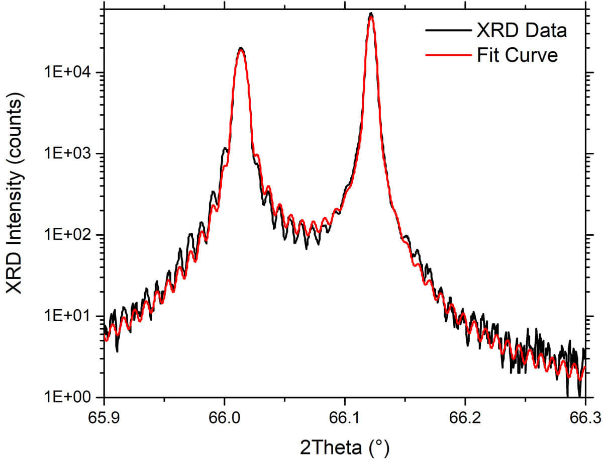
High Resolution X-Ray Diffraction
Layer lattice constant, compressive or tensile strain, and material composition are extracted using a Bruker D8 incorporating a 4x Ge monochromator for CuKɑ1 and 3x Ge analyzer crystal. Results are fit using either simple differential Bragg’s law to extract lattice mismatch, or using Bruker LEPTOS software for fitting multilayer materials with genetic algorithms. Superlattice strain, period, and total thickness are also extracted through analysis of satellite and pendellösung fringes.
Other Metrology Tools
- Hall Effect for doping concentration, mobility and resistivity (Accent HL5500PC)
- Deep Level Transient Spectroscopy using a Zurich Instruments MFIA digital lock-in amplifier for material quality assessment via Shockley-Read-Hall type traps.
- Photoreflectance (modulation spectroscopy) via a Princeton Instruments Acton Series SP-2357 Spectrometer for precise identification of band structure, internal electric fields, crystallinity and strain.
- Cryogenic Measurements (10K-500K) for any of the above metrology tools via a Cryo Industries He recirculating cryostat or Janis variable temperature micro-probe station
Pricing
Total price is based on tool utilization, substrate and materials costs, and staff time which is dependent on the complexity of the growth recipe required.
- A full platter of 3 x 2” simple GaAs diodes, LEDs, or solar cells starts around $2,500.
- A material calibration on GaAs wafer starts around $1,500.
- Both estimates above include initial setup and staff time required for new recipes. Repeating existing runs would be at a lower cost.
Request for Quote
Please contact Dr. Seth Hubbard to discuss your needs and begin a quotation for services.