In the chips
Semiconductor industry turns to RIT for good science and great people
A. Sue Weisler
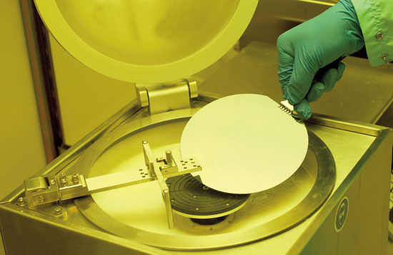
A silicon wafer being prepared in RIT’s Center for Nanolithography Research.
Students at work in RIT’s Center for Nanolithography Research are making big discoveries in a very small world. The researchers have succeeded in producing a 26-nanometer image resolution smaller than one-twentieth the wavelength of visible light. “That’s a world record in resolution,” says Bruce Smith, director of the center and Intel Professor of Research/Technology. The technique, called evanescent wave lithography, is the latest area of exploration in the center’s ongoing research to push optical imaging in microlithography beyond the limits of classical physics. “Evanescent wave lithography holds great promise,” says Smith. “The results are very exciting as images can be formed that are not really supposed to exist.” The development could be of great importance to the computer chip industry – a realm where smaller is always better.
Since the first primitive integrated circuit was produced in 1958, the industry has relied on optical technology for the precise, microscopic imaging crucial to production of chips. As chips have become smaller and more complex, the physical limits of optics have been stretched to the breaking point. “Progress in micro- and nanolithography is based on pushing the extremes of the optical resolution limit,” says Smith. “Five years ago, there wasn’t much hope that there would be many more generations left to which optical lithography could contribute.
We thought by now we would have reached the end. There have been new technologies on the horizon, but none are ready for commercial chip production. “So, any innovations that could extend the use of optical microlithography have been worth exploring. These days, every nanometer counts.” Smaller, faster, better Chips drive the modern electronics industry. The vast assortment of ubiquitous digital devices – cell phones, iPods, personal computers, cameras, video games – were made possible by chips.
Chips have fueled giant leaps in science and medicine, and they have transformed industry worldwide. This year, global sales of chips are expected to exceed $220 billion. The industry employs more than 225,000 in the U.S. Continued growth of the industry is dependent on producing successive generations of smaller, cheaper, faster and more powerful chips – a challenge that becomes more difficult with each new generation of devices. Smith says 65 nanometer device technology is the industry norm now, with 45 nanometer being inserted over the next two years. The advent of 32 nanometer technology would carry the industry for seven to 10 years; 22 nanometer, 10-plus years. “That’s possible,” Smith believes, “but that’s probably the end of the road as we know it for conventional lithography.” Several years ago, Smith and his team began exploring the potential of liquid immersion lithography. The process, based on a century-old science developed for improved visibility in microscopes, uses a layer of water to help focus the image. The team was able to produce resolution as small as 31 nanometers. These findings were first presented at a 2002 workshop sponsored by International SEMATECH, a global consortium of semiconductor manufacturers.
The RIT work was later presented at a symposium sponsored by SPIE, the International Society for Optical Engineering, in 2004-2005. Industry publications reported the story in great detail. “We thought we were onto something, but industry wasn’t interested at first,” says Smith. Then, a major semiconductor company in Taiwan began looking into liquid immersion lithography, and the rest of the industry followed suit. The RIT team continues research in immersion lithography, investigating methods of improving results with additives to the water. At the same time, the team is pursuing work on evanescent wave lithography (see accompanying article).
Earlier this year, Smith presented that research at SPIE’s Microlithography 2006. This work also has been published in trade journals. Students first Smith doesn’t know if his team’s research will ultimately become the basis for the next generation of chip manufacturing. That would be gratifying, but it isn’t the only goal of the Center for Nanolithography Research. He does know that the work in the labs is tremendously valuable for students. The team consists of six to eight undergraduate and graduate students from the College of Science and the Kate Gleason College of Engineering. Some students stay for a few quarters; others, working on doctoral degrees, may stay for several years. Anatoly Bourov, an imaging science Ph.D. candidate who came to RIT in 1993 from Leningrad, is a senior member of the team. “RIT sort of sucked me in,” he says. “I came for a one-year exchange program and stayed.” Originally interested in astrophysics, he discovered microelectronics and earned a master’s degree in that subject. “Lithography is the discipline where the boundaries get pushed the most,” says Bourov. “For a physicist, that is irresistible. The whole thing gets turned on its head every few years. That’s what keeps things interesting for me.” Although Smith and his group have freedom to explore ideas that don’t necessarily have any commercial application, they also are involved in applied research with a number of partners. The center has received substantial funding from organizations including International SEMATECH, the Defense Advanced Research Projects Agency (DARPA), Semiconductor Research Corp., IBM, Intel Corp., and ASML Holding NV. Scientists and engineers from top companies and industry organizations are regular visitors to the center.
This past summer, the group moved into larger quarters in RIT’s $30 million IT Collaboratory research building, a New York State Strategically Targeted Academic Research (STAR) Center. “RIT’s leadership in the field of nanolithography is an example of the scientific expertise we are building in New York state,” says Michael J. Relyea, executive director of the New York State Office of Science, Technology and Academic Research (NYSTAR). “Our investment in the IT Collaboratory will help the state expand its competitive edge in the arena of high-technology research. We’re also developing the highly skilled personnel needed by top science and technology companies.” The nanolithography center’s partners turn to RIT for both research and talent. “We receive support from the industry because they’re interested in the research, and because they like our students,” says Smith. “We’ve got a great reputation in this field. Our graduates are out in industry working at very senior levels.” For example, Yongfa Fan ’06 (Ph.D., microsystems engineering), who worked at the center for three years, is now a senior technology development engineer at Intel in Santa Clara, Calif. – where he often runs into other RIT grads. “I feel very comfortable here,” says Fan, a native of China. “What I learned at RIT I can apply to the work I’m doing at Intel. The Nanolithography Center is a world-class research facility. At Intel, I’m working on the same topics as at RIT. That’s what got me here.” RIT is among the top schools in the field, says Will Conley, a 25-year industry veteran who holds the title of “distinguished member of the technical staff,” Freescale Semiconductor Inc. (formerly part of Motorola). “There are a number of conferences in the industry, SPIE (International Society for Optical Engineering) being the big one,” says Conley. “A few schools always present papers, and RIT is one of them. That’s one way to gauge the quality of the work.”
Conley and Smith have known each other for more than 20 years, and have worked together on several projects through SEMATECH. He holds Smith in high regard. Conley notes that in 2004, Fan won the award for best student paper at the SPIE Microlithogaphy 2004 symposium. The prize goes to the student who can demonstrate scientific excellence in presentation, scientific rigor, writing, and the importance of the research in question to the lithography community. “It’s highly competitive,” says Conley. “Winning that is quite a testament.” Smith says the breakthrough work at the Nanolithography Center is a testament to the quality of the students. “To work in this field, you need to be a good engineer and a good scientist,” he says. “It’s very lab intensive, and the best students want that, they want to work with the technology. The technology has advanced, but our students are prepared. Our people out of this program are really on the cutting edge.”
Recommended News
-
April 24, 2024
!['David Munson, Jr., RIT President, stands on the second floor balcony of the SHED holding a portrait that shows the renderings before it was built. ']()
RIT President David Munson to step down in 2025
Spectrum News features David Munson's retirement plans for 2025, emphasizing his impact on RIT's growth in enrollment, research funding, and global presence. -
April 24, 2024
!['A blurry image of a leafy green wooded area']()
Nearsightedness is at epidemic levels – and the problem begins in childhood
The Conversation talks to Andrew Hebert, professor in the Department of Psychology, about the global rise of myopia and its causes, including increased screen time and reduced outdoor exposure.
-
April 24, 2024
!['a colorful 3 D image of the southern ring nebula appears in a black sky.']()
See the Southern Ring Nebula in 3D
Universe Today highlights the research led by Joel Kastner, professor in the Chester F. Carlson Center for Imaging Science, on the Southern Ring Nebula's dual-ring formation and the possible role of a second star.
-
April 24, 2024
!['David Munson, Jr., RIT President, stands on a balcony on the second level of the SHED.']()
RIT President Munson to retire
The Rochester Beacon covers David Munson's retirement announcement, highlighting his transformative impact on the university's creativity, innovation, and academic excellence.