RIT upgrades clean room capabilities
RIT engineering laboratory receives high tech system from Heidelberg Instruments to improve lithographic process for semiconductor fabrication
RIT recently installed a high tech laser lithography system in the Semiconductor and Microsystems Fabrication Lab to advance semiconductor research and development.
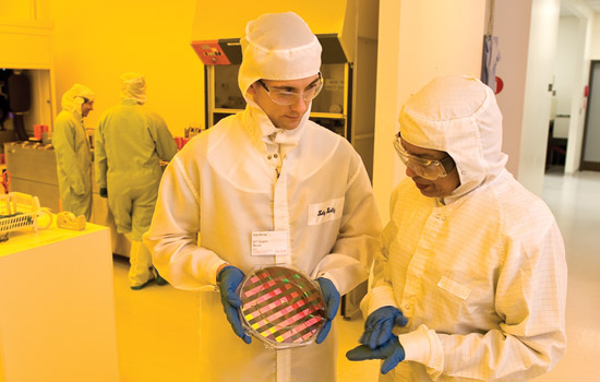
Rochester Institute of Technology recently installed a high tech laser lithography system in the university’s Semiconductor and Microsystems Fabrication Lab to advance semiconductor research and development. The system, a DWL66+ from Heidelberg Instruments, is capable of photo-mask fabrication and direct-write lithography applications—the complex process of imaging silicon wafers with microelectronic design patterns for integrated circuits.
Installed in RIT’s Semiconductor and Microsystems Fabrication Lab (SMFL), the new equipment will be used as part of several key research initiatives at the university in the areas of solar and fuel cell technology, nano-photonics and novel nanomaterials, as well support students in undergraduate and graduate programs in microelectronic engineering, and a doctoral program in microsystems engineering.
The new equipment, valued at more than $500,000, was funded in part by the National Science Foundation through its Major Research Instrumentation program for: “Acquisition of a direct-write laser system for innovations in electronic and photonic device design.”
Lithography, also referred to as photolithography, is a multi-step precision process to build, layer-upon-layer, the electronic circuitry on silicon wafers that is then used as the basis for electronic devices. The new system has several advantages over traditional proximity or projection optical lithography, said Karl Hirschman, SMFL director and professor of microelectronic engineering in RIT’s Kate Gleason College of Engineering.
“This system has the ability to handle a variety of substrate shapes and sizes, make on-demand pattern changes, and implement pattern variations within a sample. This research-scale system has wonderful flexibility and is a perfect fit for our facility,” said Hirschman. “DWL patterning can be intermixed with e-beam or optical exposure levels, providing design flexibility on pattern transfer processes. The DWL also offers new capabilities in lithography that are not possible with our other imaging systems.”
With more than 10,000 square feet of clean room space, the SMFL is equipped with micro-fabrication and metrology equipment to support research programs in semiconductor materials and devices, nano-electronics, MEMS devices and sensors, photonic devices and nanomaterials. All these systems will be utilized as part of RIT’s role in AIM Photonics, a New York-based consortium, led by SUNY Polytechnic, Rochester Institute of Technology and the University of Rochester, to focus on advancing integrated photonics, technology essential to the nation’s manufacturing capabilities in such areas as high-speed data and telecommunications.
About Heidelberg Instruments, GmbH: With an installation base of over 650 systems in more than 50 countries, Heidelberg Instruments Mikrotechnik GmbH is a world leader in production of high precision maskless lithography systems. Due to their flexibility, these systems are used in research, development and industrial applications for direct writing and photomask production by some of the most prestigious universities and industry leaders in the areas of MEMS, BioMEMS, Nano Technology, ASICS, TFT, Plasma Displays, Micro Optics, and many other related applications.
Recommended News
-
April 17, 2024
![a generated image of the new main concourse of a staium is displayed with the field to the left and a concession stand to the right.]()
RIT to break ground on new athletic stadium
Rochester Business Journal talks about the new athletics stadium being built on the RIT campus.
-
April 17, 2024
![Three biologists in a wooded area gaze up toward the treetops, looking for birds.]()
Should We Change Species to Save Them?
The New York Times cites a paper co-authored by Evelyn Brister, professor in the Department of Philosophy, about Conservation science.
-
April 17, 2024
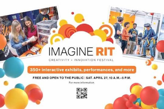
![a poster showcasing colorful balloons and an Imagine RIT banner is displayed with the date and time of the event.]()
WHY ROC: Imagine RIT Creativity and Innovation Festival
WROC-TV talks to Ann Ielapi, senior director of events and conferences for Government and Community Relations, about the upcoming Imagine RIT festival.
-
April 17, 2024
![a hand in a blue glove is holding a test tube containing large amounts of microplastics.]()
New microplastics research hub aims to unravel health impact in changing climate
RIT is spearheading a transformative $7.3 million research hub in collaboration with the University of Rochester. The center will study the lifecycle of microplastics, including its origin as plastic waste, distribution, and movement in the Great Lakes freshwater ecosystem.