Research
Epitaxial Integration of III-V Nanostructures
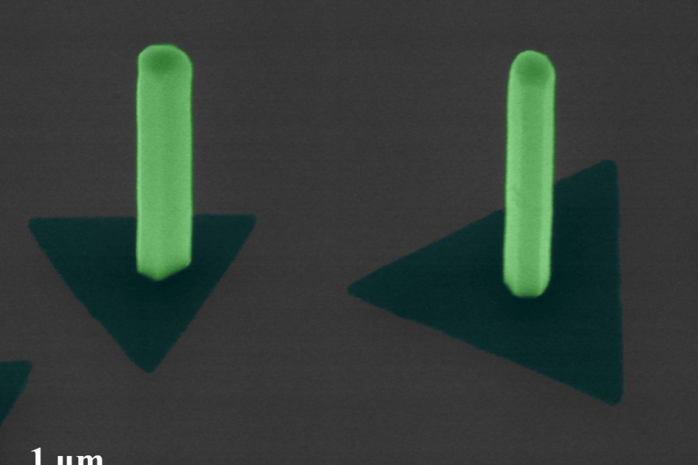
Selective Area Epitaxy on Foreign Substrates
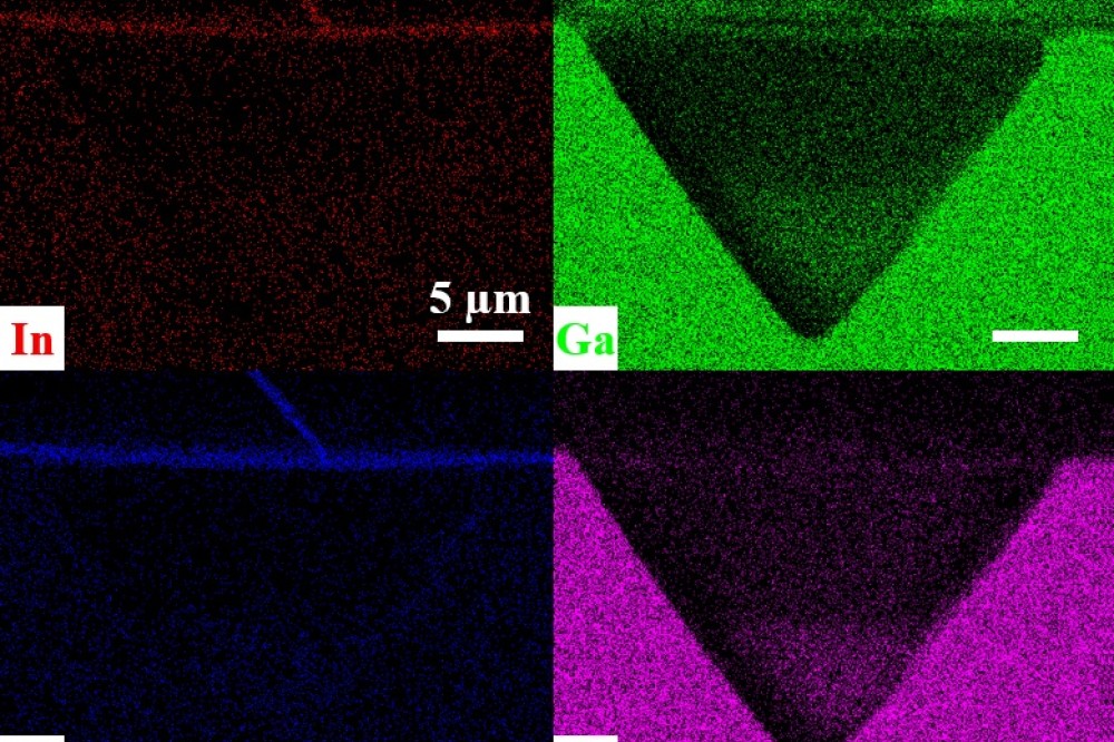
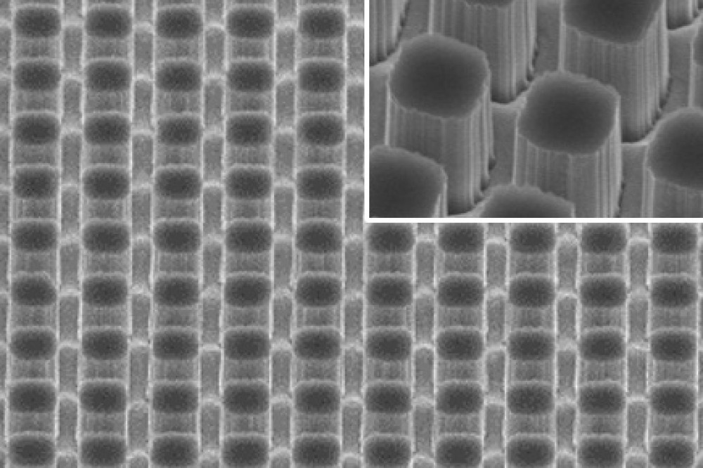
The growth of various nanostructures, including nanowires and nanofins, by metal-organic chemical vapor deposition (MOCVD) is investigated through a unique crystal synthesis process known as selective area epitaxy (SAE). The SAE method relies on an oxide template with predefined windows that specify the location of preferential epitaxial atomic assembly. Growth rate enhancement, as defined by the oxide template, allows for the controlled epitaxy of arrays of vertical, III-V compound semiconductor nanostructures without the use of foreign catalytic or seeding agents. Based on the SAE technique, the EINS lab has demonstrated growth of InAs, InGaAs, GaAs, GaAsP, and GaP nanowire and nanofin arrays on Si substrates with 100% yield over large, wafer-scale areas. Our current projects aim to understand the growth kinetics of III-V nanosystems interfaced with Si and 2-dimensional nanomaterials such as graphene and monolayer transition metal dichalcogenides; to characterize the novel material properties offered by these hybrid nanosystems; and to demonstrate their utility in innovative photovoltaics and optoelectronics solutions.

Nanofabrication by Metal-Assisted Chemical Etching
MacEtch of III-V Compounds Using Alternative Catalysts
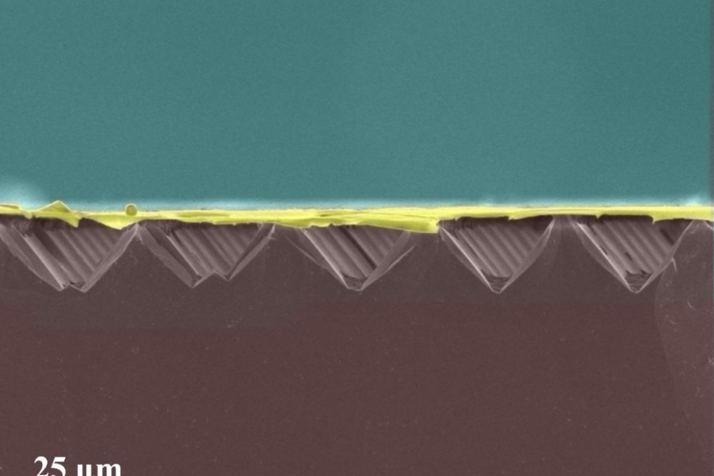
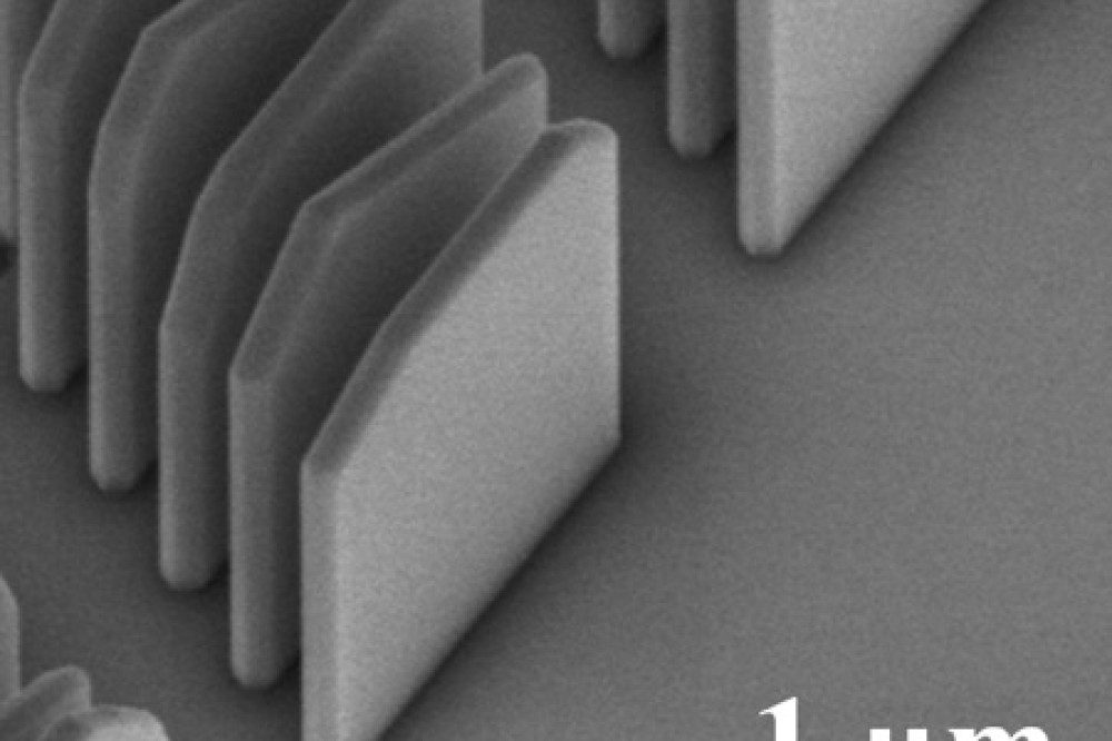
Metal-assisted chemical etching (MacEtch) is an anisotropic, solution-based nanofabrication process that combines the benefits of conventional wet-etching and plasma-based ion etching. The MacEtch process relies on site-specific, catalytic oxidation of a semiconductor surface by a patterned noble metal layer, followed by preferential dissolution of the selectively oxidized regions. Continuous repetition of oxidation-dissolution cycles in a single MacEtch bath results in the metal layer sinking into the semiconductor such that vertical nanostructures are left in the path of the metal layer, having geometries that are complementary to the geometry of the patterned metal. In the EINS lab, we are interested in exploring the fabrication of III-V semiconductor nanostructures using non-conventional metallic catalysts composed of carbon-nanotubes and graphene. In this manner we define novel nanofabrication paradigms that enable low-cost and clean alternatives to conventional ion-based etching procedures, offering high-aspect ratio features with atomically-abrupt sidewall termination. Novel device applications in high-efficiency solid-state lighting and tri-gated nanofin-based field effect transistors have already been demonstrated using on MacEtch fabrication.