Equipment
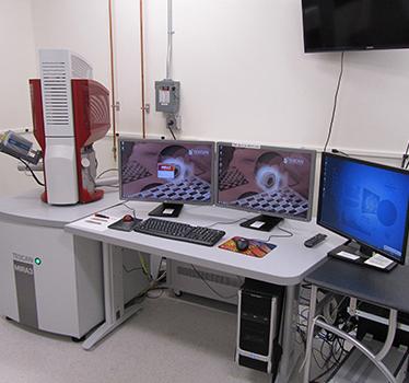
Tescan Mira3 Scanning Electron Microscope
This new microscope was installed in late 2015. It uses a field-emission electron gun to achieve 2-nm resolution at 30 kV. The chamber can accommodate specimens with a maximum diameter of 100 mm and about 30-mm thick. It operates between 0.5 and 30 kV, and has beam deceleration technology to enhance resolution at low operating voltages. Magnification is continuously variable up to 1 million. The microscope is fully digitally controlled for easy and dependable performance. It has both secondary and back-scattered electron detectors. Attached to the microscope is a Bruker energy dispersive spectrometer. This allows for compositional analysis in field-of-view, spot or small area, linescan, and mapping modes. Using the latter mode, the user can determine the spatial distributions of the elements in the sample. Quantify options are available in all modes for the quantification of elements present.
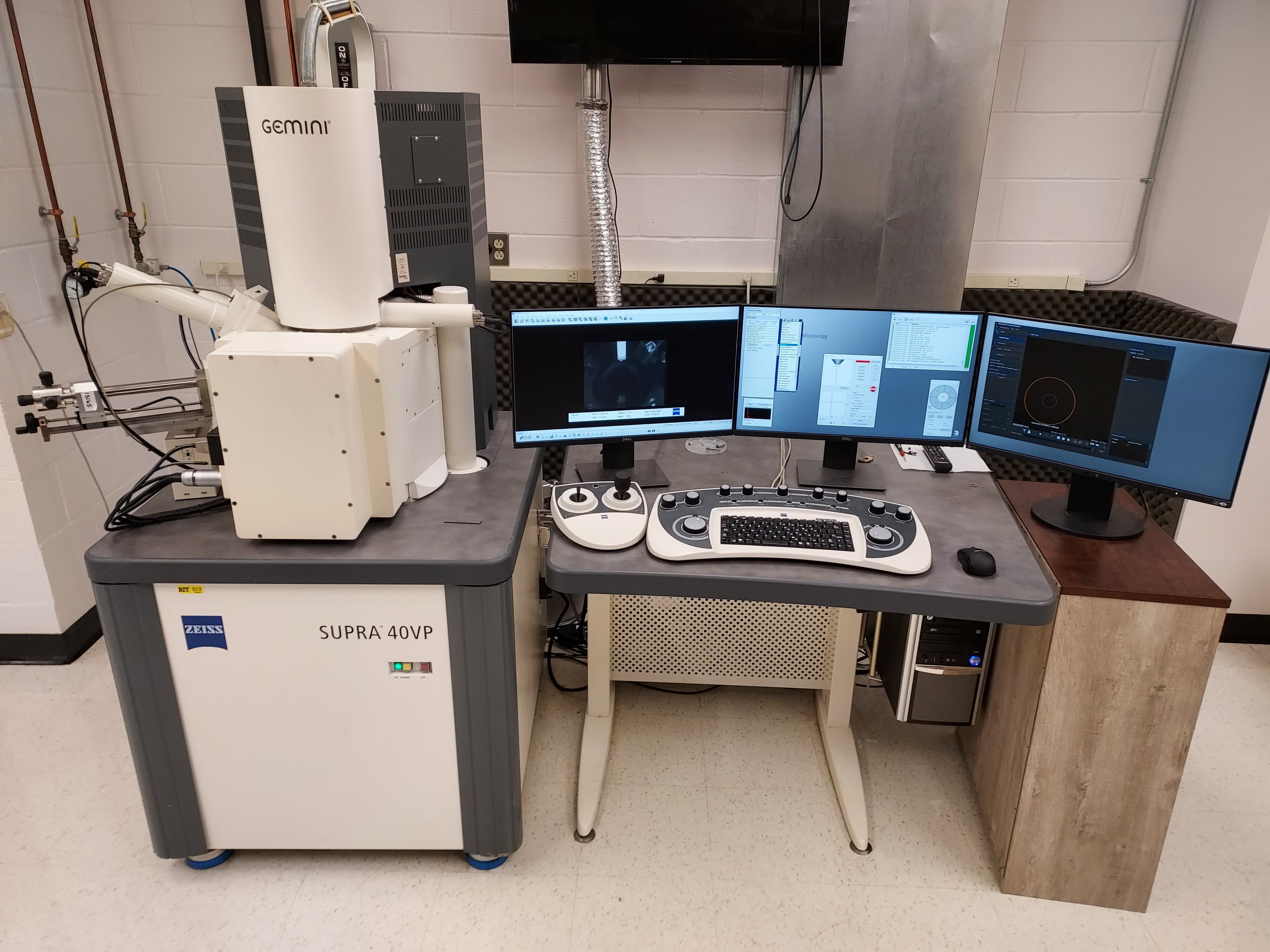
Zeiss Supra 40 VP Scanning Electron Microscope
This microscope uses a field-emission electron gun and operates between 1 and 30 kV. Specimens of a maximum diameter of 100 mm and up to 45 mm thick can be used. The SEM has a variable-pressure (VP) mode which allows non-conductive samples to be imaged without additional conductive coating. There are five detectors available: secondary electron, in-lens secondary electron, VP, backscattered electron, and STEM for imaging transmitted electrons. The SEM also has Atlas 5 software for creating comprehensive, multimodal images with a sample-centric correlative environment. This is especially useful for array tomography where imaging over several hours is needed, along with autofocusing and autostigmation.
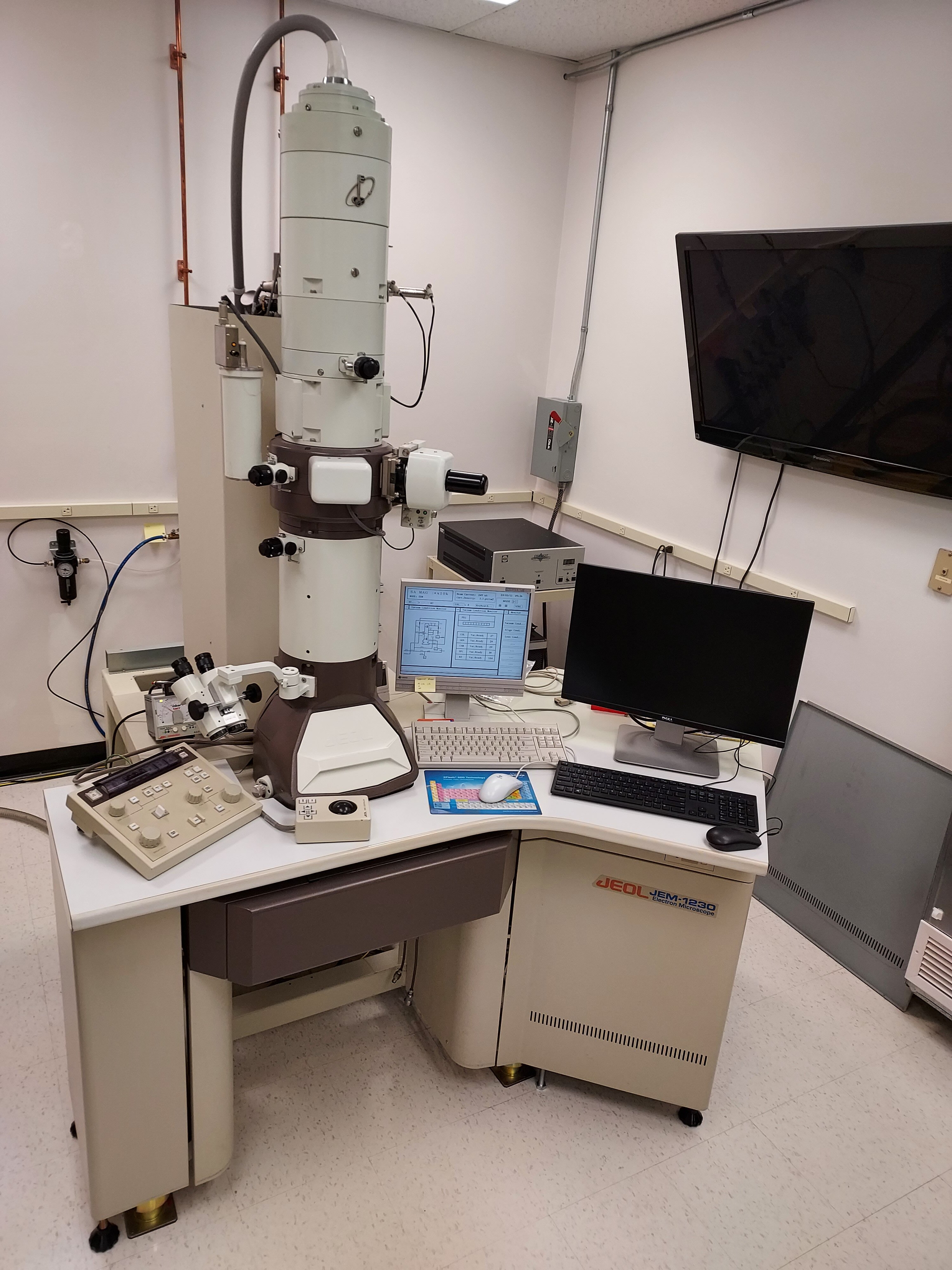
JEOL 1230 Transmission Electron Microscope
This TEM is optimized for soft materials – biological samples, and organic and polymer films. It operates between 20 and 120 kV and has a point resolution of 0.36 nm, using a tungsten filament. Specimen thickness can be up to about 200 nm with this microscope. It has the usual operating modes of imaging and selected-area electron diffraction. A low-temperature holder is available for beam-sensitive samples. Imaging is done digitally with a Gatan Model 894 UltraScan 1000 bottom-mount camera.
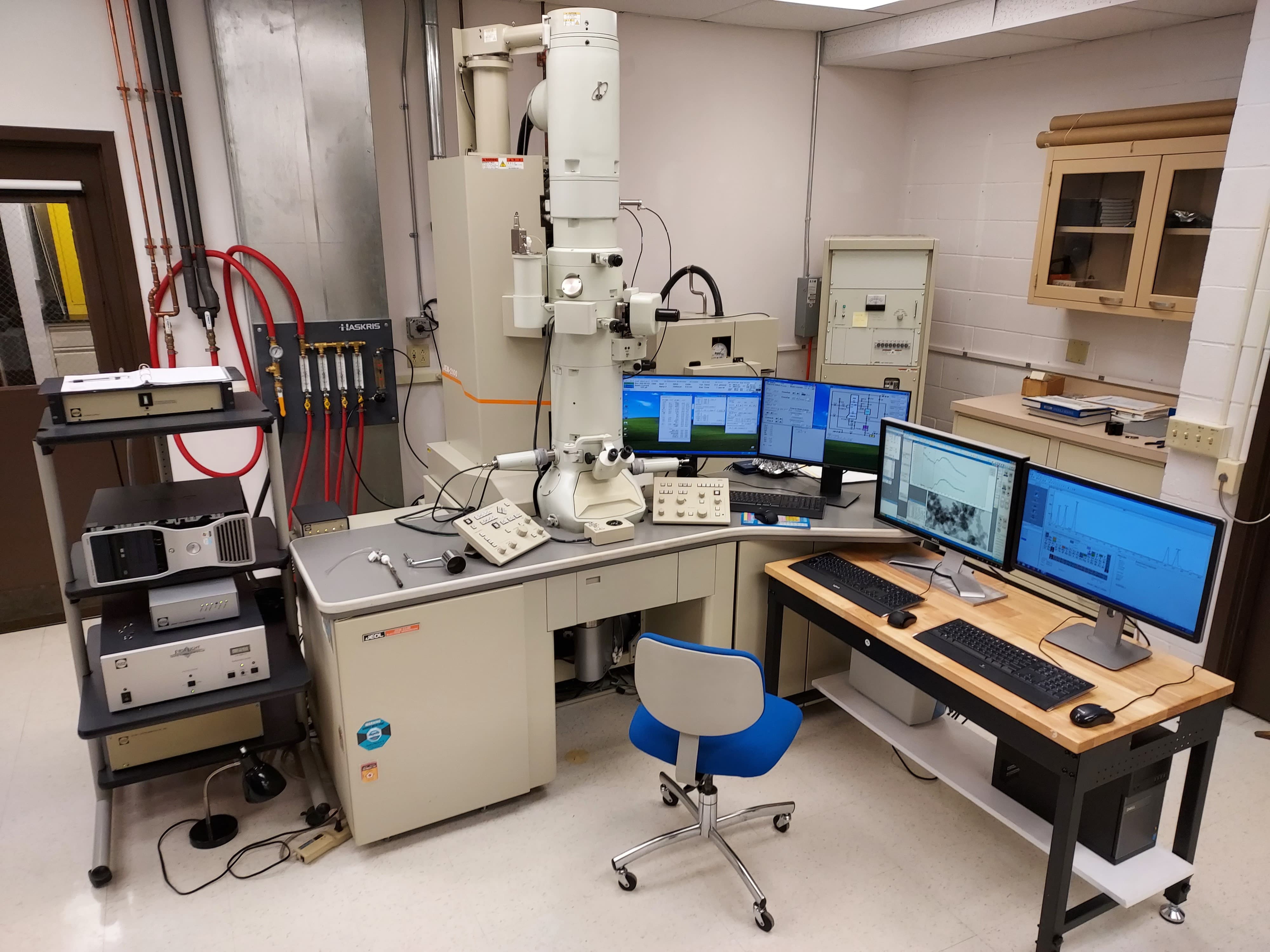
JEOL 2100 Transmission Electron Microscope
This TEM is used as a materials science characterization tool and operates between 80 and 200 kV. It is optimized for inorganic materials and has a LaB6 filament. This microscope requires thin specimens (usually less than 100 nm) and has a point resolution of 0.23 nm. Besides imaging and selected-area electron diffraction, it also has operating modes for convergent beam electron diffraction and nanobeam (down to 1 nm) electron diffraction. The TEM has both bright-field and dark-field STEM capabilities. Elemental analysis can be done in two modes: (1) An Oxford AztecEnergy X-ray microanalysis system (2) A Gatan Tridiem Electron Energy Loss Spectrometer, which enables energy-filtered TEM. Imaging is done digitally with a Gatan Orius SC 100 bottom-mount camera. A low-temperature holder is available for beam-sensitive samples.
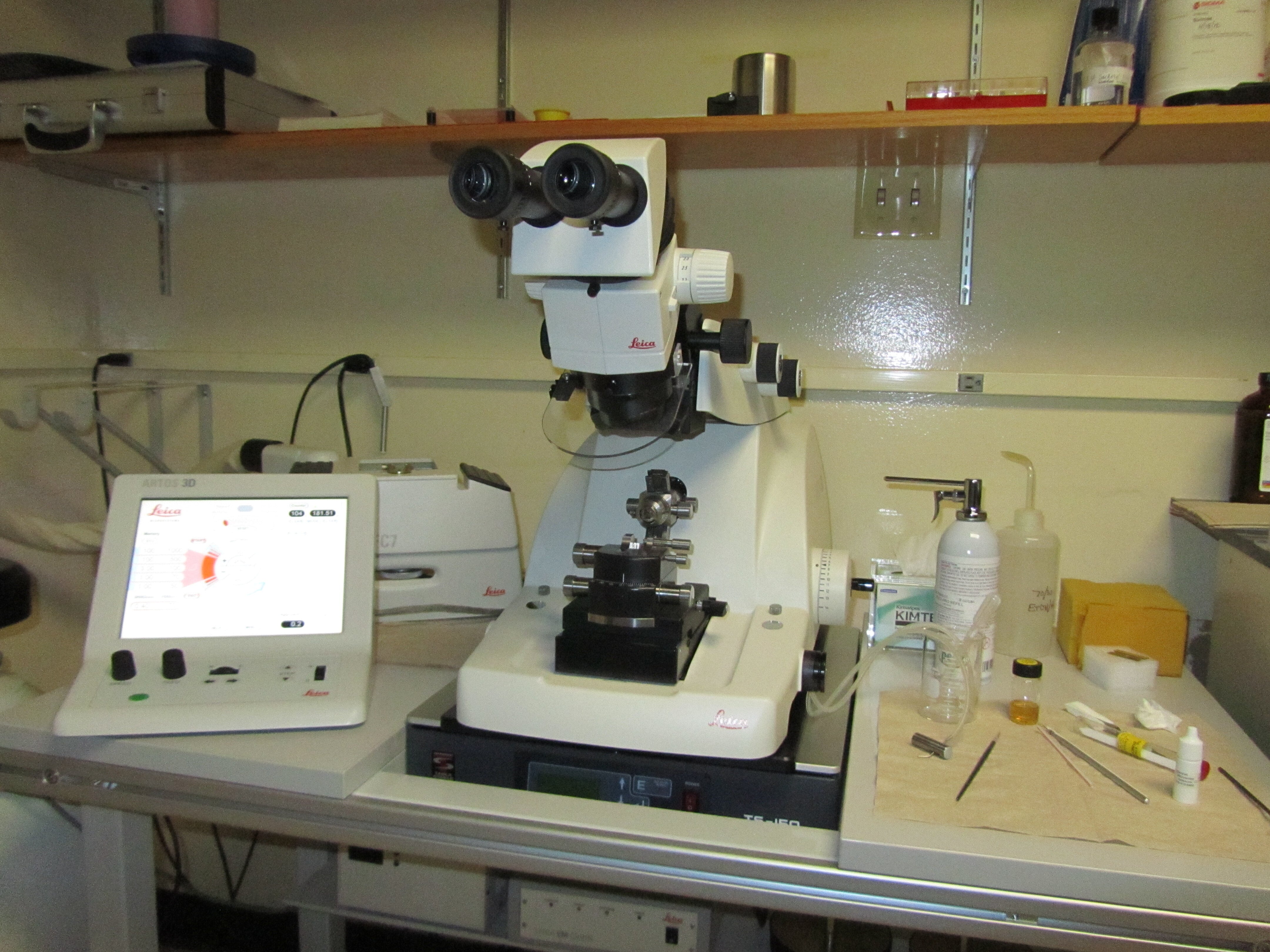
Leica Ultramicrotome
A Leica Artos 3D ultramicrotome is available to prepare thin specimens for TEM imaging and analysis. This tool is optimized for creating serial thin-section ribbons for array tomography. The ribbon collection preserves section quality for subsequent SEM imaging. A special plastic housing around the collection area minimizes the effect of air turbulence. Additionally, the ultramicrotome can work at temperatures as low as -160o C.

JEOL Ion Polisher
A JEOL Cooling Cross Section Polisher is available for preparing smooth artifact-free cross-sections for the SEM and EDS, using a broad Ar ion beam. During milling, the sample is rocked automatically to avoid creating beam striations on the polished surface. Due to the glancing incidence of the ion beam, Ar is not implanted in the sample surface. It has a cooling attachment for samples that are sensitive to thermal damage. Temperature control is possible down to -120o C.
Other Sample Preparation Equipment
For non-conductive samples intended for SEM imaging, the Lab has both an SPI sputter coater and an EMS carbon coater. For epoxy-embedded samples, the Lab has an Allied High Tech M- Prep 5 polisher that uses diamond-embedded films.