7,287,328
Methods for Distributed Electrode Injection and Systems Thereof
Patent Number
Issue Date
Inventor(s)
Michael D. Potter
Document
Download PDF for patent 7,287,328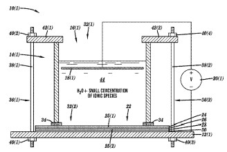
Synopsis
Patent US 7,287,328 B2 describes novel methods for injecting and trapping charge at the interface between two dissimilar insulating layers, along with applications for these charge-laden structures. This invention provides a transformative solution for various technologies requiring stable, localized charge distributions, such as micro-electro-mechanical systems (MEMS) , electrostatic generators, and sensors, by offering improved control and long-term stability of trapped charges.
A core novel aspect of this invention is the use of a distributed electrode system and a medium (e.g., fluid or solid) that comes into contact with at least one of the insulating layers. By applying an electric field across the insulating layers, charge is injected and trapped at their interface. This method allows for a more controlled and efficient injection of charge compared to traditional techniques. The patent details various configurations, including those with three layers, where a conductive base is coupled to one of the insulating layers, and the medium facilitates the charge injection from an electrode positioned above the insulating stack. The trapped charge can be monopole charge.
The commercial potential of this distributed electrode injection technology is substantial across various industries requiring advanced charge control and electret-like functionalities. Possible applications include:
-
MEMS Devices: The ability to precisely inject and trap charge within micro-scale insulating layers can enable the development of more efficient and reliable MEMS devices, such as micro-actuators, micro-pumps, and micro-sensors. This control over charge can lead to improved performance, reduced power consumption, and enhanced longevity of micro-electromechanical systems, which are increasingly critical in fields like biomedical devices, automotive systems, and consumer electronics.
-
Electrostatic Energy Harvesting: The methods described can be utilized in the development of highly efficient electret-based energy harvesters. By creating stable charge layers, these devices can convert ambient mechanical vibrations or air flow into electrical energy, providing self-powering capabilities for wireless sensors and low-power electronics in remote or difficult-to-access locations, reducing reliance on traditional batteries.
-
Advanced Sensor Technologies: The controlled injection of charge can enhance the sensitivity and stability of various sensor types, including chemical, biological, and pressure sensors. This technology could enable the creation of novel sensing platforms with improved signal-to-noise ratios and long-term operational stability, beneficial for environmental monitoring, industrial process control, and medical diagnostics.
-
Non-Volatile Memory and Data Storage: The ability to trap and retain charge at an interface for extended periods opens possibilities for novel non-volatile memory architectures. This could lead to more energy-efficient and higher-density data storage solutions, which are critical for advancements in computing and data centers.
-
Electrophotography and Printing: Enhancements in charge control on insulating surfaces could lead to improved toner adhesion and transfer in electrophotographic printing processes, resulting in higher print quality, faster speeds, and more robust imaging systems.
This patent offers a disruptive technology that enables precise and stable charge injection into insulating materials, providing a compelling opportunity for licensees to innovate in micro-fabrication, energy solutions, sensing, and data storage.