8,236,603
Polycrystalline semiconductor layers and methods for forming the same
Patent Number
Issue Date
Inventor(s)
Leslie Fritzemeier; Ryne Raffaelle; Christopher Leitz
Document
Download PDF for patent 8,236,603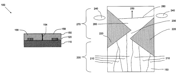
Synopsis
Patent 8,236,603 B1 describes innovative polycrystalline semiconductor layers and highly efficient methods for their formation, representing a significant breakthrough in creating high-quality semiconductor materials on a diverse range of substrates. This invention addresses the persistent challenge of high cost and limited flexibility associated with traditional single-crystal semiconductor manufacturing, unlocking new possibilities for numerous advanced electronic devices.
A core novel aspect of this invention lies in its unique approach to fabricating high-performance polycrystalline semiconductor layers on inexpensive, large-area, and even flexible substrates such as glass, plastic, or metal. This is achieved through the strategic use of an intermediate buffer layer. This buffer layer is expertly engineered to facilitate "lattice-matching" between the underlying substrate and the semiconductor material, even when their inherent crystalline structures are disparate. This critical interface mitigates stress and defects that would otherwise compromise semiconductor quality, enabling the growth of polycrystalline silicon, germanium, or gallium arsenide layers with electronic properties comparable to far more expensive single-crystal counterparts. The method's ability to deposit these layers using cost-effective and scalable vapor deposition techniques, such as sputtering, further enhances its commercial viability by ensuring low residual stress and high material quality suitable for high-volume manufacturing.
The commercial potential for this advanced semiconductor fabrication technology is immense, poised to disrupt multiple markets by enabling high-performance devices at a significantly reduced cost and in novel form factors. Possible applications include:
-
Next-Generation Solar Cells (Photovoltaics): This is a primary and transformative application. The ability to produce high-efficiency polycrystalline silicon, germanium, or gallium arsenide solar cells on flexible, large-area, and low-cost substrates (e.g., plastic films, metal foils) can drastically reduce the manufacturing cost of solar panels. This enables new product designs such as flexible solar panels for building-integrated photovoltaics (BIPV), lightweight portable chargers, and integrated power solutions for smart textiles and wearable electronics, accelerating the adoption of renewable energy.
-
Flexible and Large-Area Electronics: The technology is ideal for developing flexible displays (e.g., for smartphones, wearables, e-readers), large-area sensor arrays (e.g., X-ray detectors for medical imaging or security screening), and other printable electronic components. This opens doors to innovative product designs and more affordable manufacturing processes.
-
High-Performance Thin-Film Transistors (TFTs): It offers a cost-effective pathway for fabricating advanced TFTs on various substrates, crucial for high-resolution displays (OLED, LCD), smart cards, and integrated sensor platforms.
-
Advanced Optoelectronic Devices: The method can be leveraged to produce high-performance, low-cost photodetectors, light-emitting diodes (LEDs), and other optoelectronic components on unconventional and flexible substrates, expanding their application range.
-
Thermoelectric Devices: The ability to form high-quality semiconductor layers on diverse substrates could lead to more efficient and economically viable thermoelectric devices for converting waste heat directly into electricity.
This patent offers a foundational technology that overcomes key limitations in semiconductor manufacturing, providing a compelling opportunity for licensees to develop and commercialize a new generation of high-performance, cost-effective, and flexible electronic devices.