8,346,039
Methods for three-dimensional nanofocusing of light and systems thereof
Patent Number
Issue Date
Inventor(s)
Zhaolin LU; Ruoxi YANG
Document
Download PDF for patent 8,346,039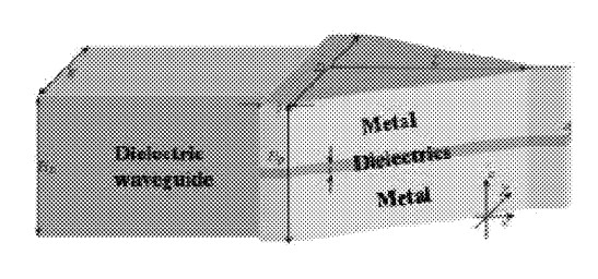
Synopsis
Patent 8,346,039 B2 describes groundbreaking methods and systems for three-dimensional nanofocusing of light, offering a transformative solution to overcome the fundamental diffraction limit of light. This invention enables the manipulation and concentration of light into extremely small, nanoscale spots, opening unprecedented possibilities across various high-tech fields.
A core novel aspect of this invention lies in its innovative hybrid waveguide structure. It combines a conventional dielectric waveguide, which efficiently guides light, with a three-dimensional metal-dielectric-metal (MDM) waveguide. The MDM waveguide can be precisely tapered in one dimension towards its output end. The process involves separately fabricating these two distinct waveguide components, followed by their meticulous alignment and bonding at one end. This integrated design allows light to be efficiently coupled from the relatively larger scale of a dielectric waveguide down to the nanoscale dimensions of the MDM waveguide. By guiding surface plasmon polaritons within the tapered MDM structure, the system effectively bypasses the diffraction limit, enabling light to be focused into a spot as small as 5 nm to 100 nm. This capability for precise, multi-dimensional nanofocusing represents a significant leap in optical engineering, facilitating light manipulation at scales previously unattainable with traditional optical components.
The commercial potential for this nanofocusing technology is substantial, particularly in industries requiring ultra-high precision in optical manipulation, imaging, and data handling. Possible applications include:
-
Ultra-High-Resolution Optical Imaging and Microscopy: This technology can enable next-generation super-resolution microscopes for advanced biological research (e.g., imaging sub-cellular structures, viruses, or single molecules in living systems) and materials science, providing unprecedented detail far beyond the capabilities of conventional optical microscopes.
-
High-Density Data Storage: The ability to focus light into nanoscale spots is critical for developing significantly higher-density optical data storage technologies, such as near-field optical data storage, enabling vast improvements in storage capacity for computing and archival purposes.
-
Advanced Nanofabrication and Lithography: In the semiconductor industry and other precision manufacturing sectors, this invention can revolutionize lithography processes, allowing for the creation of extremely fine features in integrated circuits, advanced sensors, and other nanoscale devices, pushing the boundaries of miniaturization.
-
Highly Sensitive Nanosensors: Concentrating light into a tiny, high-intensity spot at the nanoscale can lead to the development of highly sensitive optical sensors capable of detecting minute quantities of chemicals, biological markers, or even single particles, with applications in environmental monitoring, medical diagnostics, and security.
-
Enhanced Spectroscopy: The intense light-matter interaction at the nanoscale can significantly improve the sensitivity and spatial resolution of various spectroscopic techniques, facilitating more detailed analysis of materials and biological samples.
-
Integrated Photonics and Optical Computing: This nanofocusing capability is crucial for creating highly integrated photonic circuits and components for advanced optical computing and high-bandwidth optical telecommunications, enabling the miniaturization and increased efficiency of optical systems.
This patent offers a foundational technology for manipulating light at the nanoscale, providing a powerful tool for innovation across diverse high-tech sectors and presenting a compelling opportunity for licensees to lead in the development of next-generation optical solutions.