8,829,336
Nanostructured quantum dots or dashed in photovoltaic devices and methods thereof
Patent Number
Issue Date
Inventor(s)
Ryne P.Raffaelle; David M.Wilt
Document
Download PDF for patent 8,829,336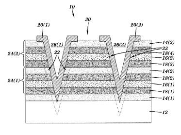
Synopsis
Patent US 8,829,336 B2 describes nanostructured quantum dots or dashes within photovoltaic devices and methods for their creation. This invention addresses a critical challenge in solar energy conversion: efficiently capturing a broader spectrum of sunlight and converting it into electricity, particularly in the infrared and ultraviolet regions where traditional silicon-based solar cells are less effective. The patent introduces a novel approach to enhance the performance of photovoltaic devices by integrating quantum structures designed to optimize light absorption and charge separation.
A key novel aspect of this invention lies in the precisely engineered arrangement of quantum dots or dashes within the intrinsic layer of a photovoltaic device. These nanostructures are formed within grooves in a semiconductor material, and conductors are placed adjacent to the entire length of the sidewalls of these grooves. This design provides:
-
Enhanced Light Absorption: Quantum dots and dashes, due to their quantum mechanical properties, can absorb photons across a wider range of wavelengths than bulk semiconductor materials. By tuning the size and composition of these nanostructures, the device can effectively capture light from different parts of the solar spectrum, including wavelengths that are typically lost.
-
Improved Carrier Collection: The strategic placement of conductors along the sidewalls of the grooves facilitates efficient collection of the photogenerated charge carriers (electrons and holes). This design minimizes recombination losses, ensuring that more of the absorbed light energy is converted into usable electrical current.
-
Scalability and Manufacturability: The method described for creating these nanostructures, including techniques like etching grooves and depositing quantum dots, appears to be compatible with existing semiconductor fabrication processes, indicating potential for cost-effective scaling and mass production.
The commercial potential for this nanostructured photovoltaic technology is significant, especially in markets driven by renewable energy and high-efficiency power generation:
-
Solar Energy Industry: The most direct application is in the next generation of solar cells. By increasing the efficiency of solar energy conversion, these devices can reduce the cost per watt of solar power, making solar energy more competitive with traditional energy sources. This is particularly relevant for applications where space is limited, such as rooftop solar installations or portable power devices, where maximizing efficiency per unit area is crucial.
-
Concentrated Photovoltaics (CPV): In CPV systems, sunlight is focused onto small, high-efficiency solar cells. This invention's ability to efficiently absorb a broad spectrum of light makes it an ideal candidate for CPV applications, which demand highly efficient cells to justify the cost of the concentrating optics.
-
Aerospace and Defense: For satellites, unmanned aerial vehicles (UAVs), and other power-constrained systems, lightweight and highly efficient solar cells are essential. The enhanced performance offered by these nanostructures could provide significant advantages in these specialized applications.
-
Consumer Electronics: Integration of these high-efficiency photovoltaic materials into portable electronic devices could enable longer battery life or even self-powered operation, reducing reliance on frequent charging.
-
Remote Power Applications: For off-grid power generation in remote areas, or in sensor networks and IoT devices, the ability to generate more power from a smaller footprint or less intense light conditions could be transformative.
This invention represents a compelling advancement in photovoltaic technology, offering a pathway to significantly more efficient solar energy conversion through innovative nanostructure design. Its ability to capture a broader spectrum of light and efficiently collect charge carriers presents a strong commercial opportunity for licensees seeking to lead the next wave of renewable energy solutions.