US 10,393,643
Optical Vortex Coronagraph Scatterometer
Synopsis
Patent US 10,393,643 B2 describes an innovative optical vortex coronagraph scatterometer designed for highly sensitive detection of scattered light. This invention provides a method and apparatus that significantly enhances the ability to measure extremely weak scattered light signals, which is critical for characterizing the quality of optical surfaces and materials.
The novel aspects of this invention stem from its unique combination of an optical vortex coronagraph with a scatterometer. Traditional scatterometers often struggle to detect faint scattering from imperfections (e.g., dust, scratches, or subsurface damage) because the intense main beam (specular reflection) overwhelms the weak scattered signal.
This invention overcomes this limitation by:
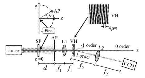
Suppressing the Specular Beam: The optical vortex coronagraph is employed to suppress the specular reflection from the sample surface. It achieves this by introducing a helical phase to the incident light, creating an optical vortex that effectively removes the central, unscattered portion of the beam.
Enhanced Scattered Light Detection: By eliminating the dominant specular component, the system allows for the detection of even minute amounts of scattered light that would otherwise be lost in the noise. This dramatically increases the sensitivity and dynamic range of the scatterometer.
Quantitative Scatter Measurement: The system is capable of measuring the Bidirectional Reflectance Distribution Function (BRDF) of the scattered light, providing a quantitative assessment of surface and material quality.
Compact Design: The patent describes a practical implementation that is relatively compact, making it suitable for integration into various inspection and manufacturing environments.
The commercial potential of this invention is substantial across industries requiring stringent quality control of optical components and surfaces, as well as in advanced scientific research.
Possible applications include:
Optics Manufacturing and Quality Control: For manufacturers of high-performance optics (e.g., lenses, mirrors, thin films for cameras, telescopes, lithography), this technology could provide an unparalleled tool for detecting manufacturing defects, subsurface damage, and surface contamination, ensuring product quality and yield.
Semiconductor Industry: In photolithography and semiconductor fabrication, the presence of even microscopic defects on wafers or photomasks can lead to significant yield losses. This scatterometer could be used for advanced defect inspection, improving manufacturing processes.
Aerospace and Defense: For critical optical systems in satellites, laser guidance systems, and high-power laser applications, minimizing scattered light is essential for performance and reliability. This invention could be used for precise characterization of space-borne optics or laser system components.
Biomedical Imaging: In microscopy and other biomedical imaging techniques, the ability to discern faint signals amidst strong background light is crucial. This technology could potentially enhance contrast and resolution in certain imaging modalities.
Materials Science Research: For researchers studying material properties, surface phenomena, or the interaction of light with matter, the high sensitivity offered by this scatterometer could enable new discoveries and advanced characterization techniques.
Display Technology: Manufacturers of high-resolution displays (e.g., OLED, LED) could use this for quality control of optical films, anti-glare coatings, and other components to ensure uniform appearance and minimize light scattering artifacts.
This invention offers a compelling solution for the advanced characterization of optical surfaces and materials, providing a significant competitive advantage to licensees in fields where precision optics and minimal scattered light are paramount.