10,409,004
Method and System to Passively Align and Attach Fiber Array to Laser Array or Optical Waveguide Arrray
Patent Number
Issue Date
Inventor(s)
Stefan Preble; Jeffrey Steidle; Michael Fanto; (Other Joint assignees)
Licensed/Under Negotiation
Document
Download PDF for patent 10,409,004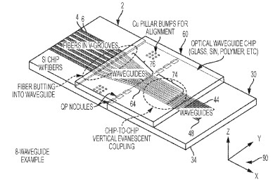
Synopsis
Patent US 10,409,004 B2 describes a method and system for passively aligning and attaching fiber arrays to laser arrays or optical waveguide arrays. This invention addresses a critical challenge in photonics and optical communications: the precise and efficient integration of optical fibers with integrated optical components.
The novel aspects of this invention lie in its passive alignment technique, which significantly reduces the complexity and cost traditionally associated with active alignment methods. The system utilizes a silicon (Si) chip with etched V-grooves designed to precisely position optical fibers. These fibers are then attached to an optical waveguide chip (which can be made of glass, silicon nitride, polymer, etc.) through a unique butt-coupling or evanescent coupling mechanism.
Key innovations include:
Passive Alignment through V-Grooves: The use of etched V-grooves on a silicon chip provides a self-aligning mechanism for the optical fibers. This eliminates the need for active, micron-level positioning adjustments during assembly, which is a major source of manufacturing cost and complexity in optical packaging.
Integrated Coupling: The design facilitates direct butt-coupling of fibers into waveguides or chip-to-chip vertical evanescent coupling between different optical components. This integration method ensures efficient light transfer with minimal loss.
Scalability: The passive alignment method is inherently scalable to high channel counts (e.g., 6-waveguide example shown), making it suitable for mass production and complex optical systems.
Robust Attachment: The system incorporates methods for robust attachment of the aligned fibers and chips, ensuring long-term stability and reliability of the optical interconnects.
The commercial potential of this invention is substantial, as it offers a cost-effective and scalable solution for manufacturing high-performance optical modules. This is particularly relevant in the rapidly expanding fields of data communications, telecommunications, and sensing.
Possible applications include:
Data Centers and High-Performance Computing: As data transfer rates increase, optical interconnects are replacing electrical ones. This technology could enable cheaper, higher-density optical transceivers and interconnects within servers, racks, and data centers, reducing power consumption and improving bandwidth.
Telecommunications Infrastructure: For fiber-to-the-home (FTTH), 5G networks, and backbone optical networks, efficient coupling of fibers to various optical components (e.g., modulators, detectors, switches) is essential. This invention could lower the cost of optical network equipment.
Sensors and Medical Devices: High-precision optical alignment is required in various sensor applications (e.g., LiDAR, gyroscopes, spectrometers) and medical imaging devices. This technology could enable more compact, robust, and cost-effective optical sensors and diagnostic tools.
Automotive and Aerospace: In autonomous vehicles and avionics, optical sensors and data links are becoming critical. This passive alignment method could facilitate the integration of rugged and reliable optical components for these demanding environments.
Quantum Computing and Photonics: Emerging fields like quantum computing and advanced photonics often require highly precise and stable optical interconnects. This invention could provide a fundamental packaging solution for such next-generation technologies.
This invention provides a compelling solution for the scalable and cost-effective manufacturing of advanced optical modules, addressing a key bottleneck in the deployment of high-speed optical systems across numerous industries.