11,353,659
Photonic Chip Features For Fiber Attachment
Patent Number
Issue Date
Inventor(s)
Mario J. Ciminelli ; Stefan Preble ; Jeffrey Steidle; Paul Thomas
Licensed/Under Negotiation
Document
Download PDF for patent 11,353,659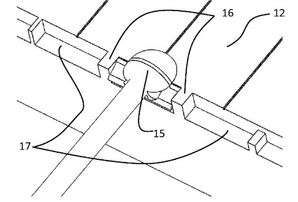
Synopsis
Patent US 11,353,659 B2 describes innovative photonic chip features designed to enhance the attachment and performance of optical fibers, specifically addressing challenges related to adhesive flow and minimizing damage during the attachment process. The invention provides structural modifications to photonic chips that facilitate more reliable and high-efficiency optical coupling.
A key novel aspect of this patent lies in its dual approach to improving fiber attachment. First, it introduces a "recessed rim" design at the periphery of the photonic chip, featuring geometric elements like trenches or barriers that effectively separate multiple waveguide locations. These features are specifically engineered to prevent the flow of adhesive material (used for bonding optical fibers) between adjacent waveguide sites. This selective containment of adhesive is crucial for maintaining optical integrity and preventing signal degradation that can occur when excess adhesive interferes with light paths or bonding areas. Second, the patent details an "optical fiber groove" with a unique flared entrance portion. This flared opening provides a larger clearance at the point where an optical fiber enters the groove, gradually narrowing to a non-entrance portion. This design minimizes the risk of damage to both the optical fiber and the photonic chip during insertion and alignment, which are critical steps in achieving low-loss optical coupling.
The commercial potential of this invention is substantial within the rapidly expanding fields of optical communications, data centers, and various photonics-enabled technologies. As data rates increase and optical interconnects become more prevalent, the demand for highly reliable, efficient, and cost-effective fiber-to-chip coupling solutions is paramount.
Possible applications include:
High-Speed Data Communications: Improving the performance and reliability of optical transceivers in data centers and telecommunication networks. Enhanced coupling efficiency translates to lower signal loss and higher bandwidth, which is essential for supporting increasing internet traffic and cloud computing demands.
Integrated Photonics: Facilitating the mass production and deployment of complex photonic integrated circuits (PICs) by simplifying and making more robust the fiber attachment process. This could accelerate the adoption of PICs in various applications, from LiDAR systems to medical diagnostics.
Sensors: Enabling more precise and stable optical sensors by ensuring optimal light coupling. This is relevant for environmental monitoring, industrial control, and biomedical sensing where accuracy and long-term stability are critical.
Quantum Computing and Sensing: Providing robust interfaces for quantum photonic chips, where precise optical alignment and minimal loss are crucial for maintaining quantum coherence and achieving high fidelity operations.
Aerospace and Defense: Developing ruggedized optical modules for harsh environments, where reliable fiber connections are vital for communication, sensing, and navigation systems. The damage-minimizing design and adhesive control contribute to increased system durability.
This patent offers a fundamental advancement in the physical design of photonic chips, addressing long-standing manufacturing and performance challenges in optical fiber attachment. By enabling more efficient and reliable optical coupling, it provides a pathway to unlock further innovation and scalability across numerous photonics-driven industries.