11,471,980
Method and System for Ultrafast Laser-based Material Removal, Figuring and Polishing
Patent Number
Issue Date
Inventor(s)
Lauren L. Taylor
Licensed/Under Negotiation
Document
Download PDF for patent 11,471,980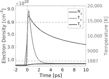
Synopsis
Patent US 11,471,980 B2 describes a method and system for ultrafast laser-based material removal, figuring, and polishing. The invention focuses on optimizing ultrafast laser processing for various materials by incorporating physical modeling to understand laser/material interaction mechanisms and the impact of laser parameters. This approach aims to achieve high-quality surface modification with minimal heat accumulation, which is a significant challenge in precision laser processing.
A key novel aspect of this patent is its integrated approach to process optimization. It involves determining a laser fluence near the ablation threshold for a given material and pulse duration. Subsequently, it optimizes the repetition rate, scanning speed, and scanning strategy to minimize heat accumulation, recommending an operable line scan overlap between 50% to 85% for achieving smooth ultrafast-laser polishing while maintaining an optic-quality surface. This level of control over laser parameters, guided by a physical understanding of the interaction, distinguishes it from conventional trial-and-error methods. The method also enables the generation of highly specific surface patterns and features with precision.
The commercial potential of this invention is substantial across industries requiring high-precision material processing and surface finishing. The ability to achieve optic-quality surfaces with minimal thermal damage opens up new possibilities for manufacturing and customization.
Possible applications include:
Optics and Photonics: Precision figuring and polishing of optical components for lenses, mirrors, waveguides, and other optical instruments. This can lead to improved performance and reduced manufacturing costs for high-value optical elements.
Semiconductor Manufacturing: Advanced patterning, etching, and surface modification of semiconductor wafers. The minimal heat accumulation is crucial for fabricating delicate microelectronic circuits without damaging adjacent structures.
Medical Device Manufacturing: Precision machining of biocompatible materials for implants, surgical tools, and diagnostic devices, where surface quality and material integrity are paramount.
Aerospace and Defense: Fabrication of high-performance components from advanced materials that require precise dimensions and superior surface finishes for critical applications.
Automotive Industry: Manufacturing of engine components, sensors, and aesthetic parts with enhanced durability and performance through precise surface texturing or polishing.
Micro-electromechanical Systems (MEMS): Creation of intricate micro-structures and devices with high accuracy and minimal material distortion.
This technology offers a pathway to more efficient, precise, and less damaging laser material processing, enabling manufacturers to meet the increasing demands for high-quality components across a diverse range of advanced applications.