12,015,105
Capacitive Control of Electrostatic Field Effect Optoelectronic Device
Patent Number
Issue Date
Inventor(s)
Matthew Hartensveld; Jing Zhang
Licensed/Under Negotiation
Document
Download PDF for patent 12,015,105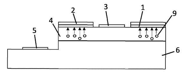
Synopsis
Patent US 12,015,105 B2 describes a method and device for the capacitive control of an electrostatic field effect optoelectronic device (EFEOED). This invention focuses on modulating charges within layers of the EFEOED by applying a positive or negative bias to a capacitively coupled plate, thereby adjusting the device's charge utilization efficiency. This approach is applicable to both light-emitting diodes (LEDs) and solar cells.
A significant novel aspect of this invention is its direct method of improving charge utilization efficiency through electrostatic field effect control, without relying on traditional current spreading layers that often introduce high resistivity and voltage drops. By applying a bias to a capacitively coupled plate, the system can either attract or repel dominant charge carriers in the underlying doped layers. For LEDs, this repulsion of dominant charge carriers leads to increased charge recombination and enhanced light emission. For solar cells, the capacitively coupled plate can simultaneously repel minority charge carriers and attract majority charge carriers, aiding in charge separation and subsequent current generation. The insulating layer in the device is designed to block current flow and has an energy band alignment that ensures minimal current leakage. This allows for precise control of charge carriers to either increase or decrease light generation or current output as needed. The ability to apply bias to the capacitively coupled plate allows for modulated intensity of charge attraction or repulsion based on the magnitude of the applied voltage.
The commercial potential of this invention is substantial across various sectors:
- LED Manufacturing: This technology offers a pathway to develop more efficient LEDs. By increasing the charge utilization efficiency, manufacturers can produce brighter LEDs with lower power consumption, which is critical for applications ranging from general lighting to display technologies and automotive lighting. Improved efficiency can lead to reduced operational costs for end-users and a competitive advantage for manufacturers.
- Solar Energy: For solar cells, the invention's ability to enhance charge separation and current generation translates to higher power conversion efficiencies. This directly impacts the economic viability of solar power, making solar panels more attractive for residential, commercial, and utility-scale installations. Increased efficiency per unit area could also lead to smaller, more powerful solar devices for various portable and integrated applications.
- Optoelectronic Components: Beyond standard LEDs and solar cells, the core principle of capacitively controlled charge modulation could be applied to a broader range of optoelectronic devices, including photodetectors, optical sensors, and specialized light sources. This allows fine-tuning of device performance for specific applications.
- Cost Reduction and Performance Enhancement: The invention’s departure from traditional current spreading layers suggests potential for simpler fabrication processes or reduced material costs, alongside performance improvements. This dual benefit of enhanced performance and potentially lower manufacturing expenses makes the technology appealing for licensing.
This invention provides a robust mechanism to optimize the performance of optoelectronic devices, offering a competitive edge through enhanced efficiency and versatility in various applications.