Design & Test
RAMLab runs a complete integrated circuit design flow in house, from schematic entry through tapeout to silicon measurement. Students take their own designs through every stage of that cycle, typically over eighteen months from architecture to measured results.
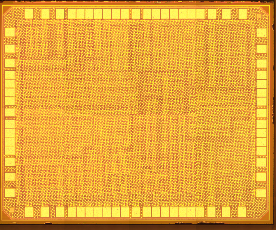
Compute and EDA
- High performance compute servers (20+ Xeon servers, 1.5 TB RAM each)
- Access to modern foundry PDKs, tapeout and fabrication facilities
- 22 nm, 28 nm, 55 nm, 65 nm and 180 nm CMOS processes
- EDA tools from Cadence, Siemens EDA (Mentor Graphics) and Synopsys
- Altium PCB designer
Test and measurement
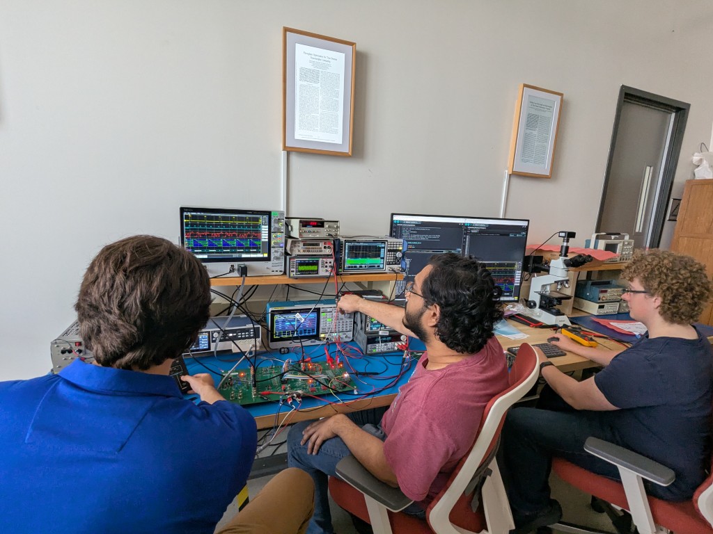
- High frequency validation bench
- 4 GHz mixed-signal oscilloscope
- 7 GHz spectrum analyzer
- Arbitrary waveform generator and RF signal generator
- Source meter, LCR meter and supporting instrumentation
- 75-inch interactive touch display
Fabrication and packaging
Our designs are fabricated at commercial foundries. On-campus facilities support device work, packaging and bring-up:
- RIT fabrication cleanroom
- RIT packaging facility
- Wafer probing setup