Research

Dr. Hubbard’s research focuses on Photovoltaic and Optoelectronic Devices, Radiation Hardened Space Power, III-V Semiconductors, and Vapor Phase Epitaxy.

Our activities encompass materials synthesis, device fabrication, material and device modeling, as well as characterization both at the electrical and materials level. Specific expertise lies in vapor phase epitaxy (VPE) of III-V photovoltaic devices and nanostructures, novel photovoltaic structure growth and design and all forms of photovoltaic characterization and simulation.

Interests

  • Epitaxial Crystal Growth by Metalorganic Chemical Vapor Deposition (MOCVD)
  • Semiconductor Device Design and Fabrication
  • Thin-Film Characterization Techniques
  • MOCVD System Design
  • Nano-structures (quantum wires/dots) for enhanced efficiency photovoltaic cells.
  • High Efficiency Nanostructured III-V Photovoltaics for Solar Concentrator Application
  • Growth of semiconductor nanostructures using MOVPE growth techniques
  • Novel Approaches to Power Conversion (alphavoltaics, thin-film III-Vs)
  • Nanostructured gas/chemical sensors

Current Projects

A laser being focused on a chip.

MOCVD regrowth of wide-bandgap (WBG) III-P Epilayers

The next generation of wearable devices will require small-featured displays to achieve high resolution. The micrometer light emitting diode (micro-LED) can enable near-eye displays through low power consumption, long lifetime, high contrast, enhanced response time and increased resolution. The micro-LED design proposes to significantly improve the resolution of near-eye displays since they are over 10-times smaller than conventional mm-size LED. However, the process development required to create a micro-LED damages the sidewalls and introduces defects, which degrades the light output power of these devices. As these devices reduce in size, surface states limit the light output power (LOP) at the roughened sidewalls, and the perimeter-to-area ratio must be considered. Light management through sidewall passivation, surface cleaning, and regrowth techniques are being studied to improve the LOP from these devices.

Two closeups, at different zoom levels, of quantum structured solar cells.

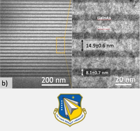
High Efficiency Quantum Structured Solar Cells

Nanostructured quantum well and quantum dot III–V solar cells provide a pathway to implement advanced single or dual junction photovoltaic device designs that can capture energy typically lost in traditional solar cells. A strained quantum well superlattice solar cell recently fabricated and tested at RIT achieved an AM1.5 efficiency greater than 30% with great promise for further improvements. A major opportunity exists to advance solar power generation and resiliency by exploring QW devices, increasing their TRL, and transferring technology to industry. QW structures can be implemented into many types of solar cell devices, potentially increasing power by up to 25% for satellites at end-of-life and 10% for aircraft, compared to state-of-practice (SOP) 3-junction devices.

A diagram of a solar cell and how it works as an optical data communication device, receiving signal, and energy at the same time.

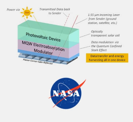
Solar Cell Integrated Modulating Retroreflector

One of the major drivers in recent and future satellite research is the need for more satellites and increased communication speed, especially with the emergence of proliferated low-Earth orbit (pLEO) constellations. The aerospace industry is now trending towards using optical data communication, as opposed to legacy radio frequency (RF) communications. III-V based multiple quantum-well (MQW) based electroabsorptive modulators (EAMs) have been used to demonstrate high speed, high ON/OFF keyed FSO communication. III-V semiconductors are also the class of materials typically used for photovoltaic (PV) arrays for satellites due to their exceptional efficiencies of upwards of 35% and ability to be made thin, flexible, and lightweight. PV has the potential to be an enabling platform for integrating an optical communication component for free space optical (FSO) systems, such as an EAM, due to the large aperture provided by the solar panels for a satellite and the already existing solar cell architecture. Combining an EAM with the large area PV array reduces the pointing accuracy required for FSO. Additionally, this reduces the SWaP of the system by hybridizing power and communication into one package. Our team is working on heterogeneous integration of FSO systems with PV using both mechanical and moonlight approaches.

Sonic wafers.

Sonic Wafering of III-V substrates for High Efficiency Cells: A path to <$0.50/W

III-V solar cells have long-demonstrated the highest power conversion efficiencies of any material system. However, a recent techno-economic analysis placed the fraction of GaAs single-junction photovoltaic device cost due to the substrate as high as 84%. Partners at Arizona State University and the National Renewable Energy Laboratory have been developing a wafer spalling technique that could have a direct impact on this high cost by cyclically removing the product device from the substrate, and enabling substrate re-use for additional PV manufacturing. The technique combines the prestressing of a GaAs crystal at low temperature with acoustic waves to controllably propagate a crack at low velocities. RIT is collaborating with our partners in the investigation of metalorganic chemical vapor deposition of GaAs on spalled substrates and fabrication of low cost, large area III-V solar cells.

A mockup of a two rovers on the moon, using a high efficiency lasers to communicate.

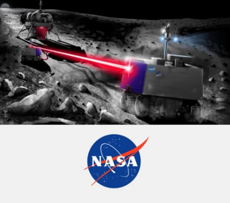
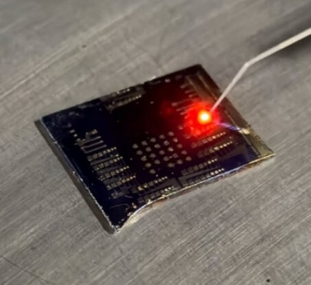
High Efficiency Laser Power Beaming Receiver for Lunar and Extraterrestrial Exploration

One of NASA’s strategic goals is a return to cis-lunar space and establishment of permeant manned and unmanned scientific installations on the lunar surface.  Study of so-called “cold traps”, or permanently shadowed lunar craters near the north and south polar regions is of high importance since they may contain water ice, useful for both scientific study of the early history of the moon-Earth system as well as a potential source of hydrogen and oxygen for use in habitation or as fuel. However, the temperature of the lunar surface in the dark averages near 140K, and may be closer to 25K inside permanently shadowed craters. Currently, operational energy demands of these unmanned/autonomous lunar systems would be dependent on on-board energy storage of fuel or batteries which impose a time limit on operation. However, through appropriate wireless laser power beaming, the power reserves of a system could be extended indefinitely. Long-range power transfer in the far-field regime (meters to kilometer range) requires directional and concentrated sources of radiation available using lasers. Laser power beaming requires smaller size transmitters and receivers compared to microwaves; the systems can be built using all solid-state components; they have higher immunity to electromagnetic interference; and they have the potential for conversion efficiency over 70%. RIT is working on a number of goals to both grow multijunction power converters for 1064 nm operation as well as combining our converters with data transmission/reception devices to further impact SWaP.

A mockup and diagram of a cubesat using an RTG.

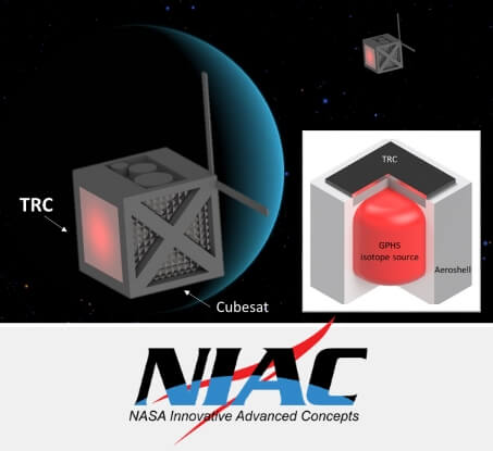
Radioisotope Thermoradiative Cell Power Generator

This NASA Innovative Advanced Concepts (NIAC) project investigates a revolutionary power source for missions to the outer planets utilizing a new paradigm in thermal power conversion, the thermoradiative cell (TRC). Available solar energy decreases as the square of the distance from the Sun, resulting in very low irradiance at the outer planets making photovoltaics infeasible. Instead, current missions beyond Jupiter are powered by radioisotope thermoelectric generators (RTG) which can only convert about 6% of the thermal energy produced by their expensive, and difficult to produce, plutonium heat sources. The TRC is a new alternative in solid state thermal to electrical energy conversion which operates like a solar cell in reverse. Photons are spontaneously generated by recombination of charge carriers inside the TRC diode which are rejected into cold outer space, thus cooling the TRC. A radioisotope heat source maintains the TRC temperature, allowing this radiative emission to drive a current inside the device and provide power to an external load. Low bandgap semiconductor materials are necessary for operation, leading RIT to investigate InAsSb at 0.28 eV. Our work suggests power conversion efficiencies in excess of 12% are possible in this system, doubling that of current state-of-the-art RTGs. Higher power conversion efficiency will enable better utilization of plutonium, and the reduced form factor of the TRC versus the RTG will allow use in many small cubesats as opposed to one large craft, increasing mission capabilities.

Closeups of laser bars for print and a release layer etched laser bar.

Hybrid and Heterogeneous Integration of PICs for RF Photonic Imaging Systems

The goal of this collaborative effort is to develop high-density heterogeneous and hybrid photonic integrated circuit (PIC) packaging techniques to support the demonstration of an analog RF photonic imaging system-in-a-package. Our team is primarily contributing to developing hybrid and heterogeneous integration of PIC materials to realize a multi-chip electro-optic system on-chip using Micro Transfer Printing (µTP) and photonic wire bonding (PWB).

Select Past Projects

This $1.75M capital equipment project was for the design and implementation of a III-V material growth facility using Metal Organic Chemical Vapor Deposition (MOCVD). The equipment, facility upgrades and personnel support for this project was funded in part by the National Science Foundation (NSF), Empire State Development (NYS), the Office of Naval Research and the Rochester Institute of Technology (RIT), VP of Research and the RIT-Kate Gleason College of Engineering. The system is installed in the Semiconductor and Mircrosystems Fabrication Laboratory (SMFL).

The MOCVD is devoted to the growth of III-V materials and devices containing As, P and Sb. The MOCVD has proven to provide the variety of materials, thickness, composition, and doping control necessary for the various nanomaterials and nanostructures used in our research.

Current programs that utilize the MOCVD include the development of quantum wells, wires and dots for high efficiency solar cells, III-V materials integrated with silicon based nanophotonics, next generation imaging array detectors and nanostructured III-V devices for radioisotope micro-batteries for health and security related microsystems. Adding this on-site III-V growth capability complements RIT’s outstanding processing and characterization facilities and provides our students with state-of-the-art tools to excel in their chosen fields of study.

This project sheds light on the technology and device physics of next generation quantum dot solar cells, leading to an intermediate band solar cell. One facet of the research was focused on QD materials systems with improved bandgap and little valence band offset for IBSC application. The other focus was on a doping superlattice nipi devices, which allow for longer carrier lifetime, improved absorption coefficients and high QD doping levels. Project results led to significant advances in epitaxial growth of QD, QW and strain balancing systems for both bandgap engineering of tandem devices as well as intermediate band solar cell designs. Specific advances include demonstration of current enhancement in an InAs QD enhanced GaAs solar cell, demonstration of InGaP solar cells with InAs QDs, radiation hardening of quantum enhanced multijunction solar cells, understanding of the role of the device electric field on carrier escape from QDs and development of multiple simulation tools for QW and QD enhanced solar cells.

As well this project resulted in the first experimental demonstration of a doping superlattice solar cell. These devices were shown by both simulation and experimentally to have enhanced carrier collection under extreme radiation conditions due to drift dominated collection. This project resulted in 8 journal articles, multiple conference proceedings and invited talks and 2 PhD theses.

The Strain Balanced Quantum Dots for High Concentration Solar Photovoltaics projects provided insight into the fundamental material aspects of using nanomaterials for bandgap engineering multi-junction solar cells or for advanced concepts such as the intermediate band solar cell (IBSC). The overarching goal of this project is to addresses the need for future high-efficiency solar cells for either space photovoltaics (PV) or high concentration grid-tied solar farms. Specifically, the project has made advances in regards to strain balancing of InAs quantum dots using GaAsP, developing a fundamental theory for strain balanced QD superlattices. This resulted in a nanoHUB application to predict strain balancing thickness and maximum number of QD layers that can be stain balanced before onset of plastic relaxation. Improvements to understanding of QD strain balancing resulted in two record solar cell achievements: the highest reported open circuit voltage for an InAs QD solar cell and demonstration of a record 0.5% absolute increase in conversion efficiency for QD based solar cells.

As well, in collaboration with a multi-junction solar cell manufacture, we were able to demonstrate for the first time that InAs QDs can be used for bandgap engineering of the middle GaAs cell in an upright triple junction solar cell configuration on Ge substrates. In addition to strain balancing, this project has also enhanced our understanding of QD growth mechanisms by metal organic vapor phase epitaxy using on-axis and vicinal substrates, provided theory to explain the escape mechanisms in QD solar cell and QD interaction with device electric field, and demonstrated experimentally how delta doping can be used with QDs for IBSC application. Specific to IBSC, we have used numerical k.p simulation map potential IBSC materials that are more suitable than standard InAs on GaAs systems. Options identified include GaSb QDs using GaAsSb barriers and InAs QDs using AlAsSb, AlGaAs or InGaP barriers.

InAs QDs have been experimentally demonstrated on both AlGaAs and InGaP, with AlGaAs showing the most promise, best material quality and highest electron confinement. Future work under separate funding is now concentrated on experimental demonstration of AlGaAs and GaAsSb based IBSC. Our results have been disseminated though both conference talks and proceedings, journal publications, invited talks by the PI, book chapters, software programs developed, websites and outreach activities. We have published 8 journal articles, 23 conference proceedings, 1 book chapter and a software product on Nanohub. The project supported 2 faculty members, 1 post-doctoral fellow, 2 PhD, 4 MS, 6 undergraduates and 1 high school student. One of the PhD students is now an Assistant Professor and 2 of the MS students have taken positions at US Government research laboratories. Multiple outreach activities have been conducted under this project, including solar day activities though the Imagine RIT festival, public demonstrations of solar energy at the Rochester Museum and Science Center and many ½-day solar cell camps and demonstrations to high school students in grades 9-12.

In order to achieve a high efficiency using the IBSC concept, it is vital to study a suitable material system using a systematic approach. This proposal studied a solution using a QD/barrier system of antimony-based ternary materials. III-Sb materials have bandgaps from 0.3 to 2.1 eV. Moreover these systems are predicted to have a favorable IB position in energy alignment and to satisfy most if not all of the requirements for IBSCs. Our theoretical calculations predicted that InAs(Sb) QDs in AlAsSb barriers produce close to ideal band gaps required for IBSC. Though this material system is challenging to grow and not well studied, we have made excellent progress in achieving high quality QDs array that form an intermediate band. This included a demonstration of the first ever report of InAs quantum dots on AlAsSb, successful demonstration of two-photon absorption in InAs/AlAsSb QDs and the longest wavelength (~1.8 microns) photoresponse to date reported in QD-IBSCs. This project resulted in over 20 journal and conference publications and 1 PhD thesis.

Space photovoltaics degrade under the radiation environment in space, depending on the materials and design of the photovoltaic (PV) cells. In this project we have demonstrated novel quantum well enhanced multi-junction solar cells can deliver more efficient, radiation hardened and lightweight solar cells and arrays. Standard upright triple junction solar cells with QW enhanced regions were grown and investigated under various space radiation environments, with improved end of life performance. We have also develop and provided reliable, validated computational tool for assessment and optimization of the QW enhanced technologies for space PV applications.

III-V based nanowires (NW) have promising potential in next-generation electronic, photonic, and photovoltaic device applications. However, considerable effort remains at the fundamental materials level in order to fully exploit the benefits afforded at the nanoscale. In particular, the use of core-shell NWs or hybrid organic-NW approaches for photovoltaic applications, in which the junction is radial while the optical absorption is axial, can enable high photo-conversion efficiency in low diffusion length materials (such as mismatched materials) by decoupling the optical absorption from the carrier collection. However, in all NW based devices, surface recombination and thus passivation becomes a critical issue. This projected investigated the use of InAs nanowires as the photon collection mechanism in a photovoltaic device. InAs nanowires were grown by MOCVD using multiple distinct nucleation approaches: in‐situ nucleation, Au‐nanoparticle nucleation and catalyst free nucleation using a di-block copolymer masking scheme. The nanowire density and uniformity were characterized as a function of nucleation method and substrate orientation. A novel approach to NW epitaxy was demonstrated that eliminates the need for an Au-based catalyst nanoparticle using an in-situ generated metallic nano-droplet, In addition, the PI’s also collaborated with University of Wisconsin to investigating NW epitaxy mechanisms using a diblock copolymer (DBC) nanolithography template. NWs were observed to nucleate in the DBC pattern with no misfit or threading dislocations along the length of the NW. Initial photovoltaic response was demonstrated for both nucleation methods, with promise for applications in both space and terrestrial use.