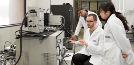
Facilities

III-V Epitaxy
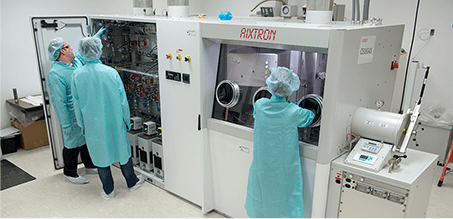
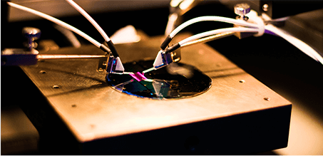
Through a recent NSF MRI award (DMR-1337592) RIT has purchased and installed a metal organic vapor phase epitaxy (MOVPE) system for growth of III-V thin film crystals and nanostructures. The equipment, shown in figure below, consists of an Aixton 3×2” Close Coupled Showerhead (CCS) metalorganic vapor phase epitaxy (MOVPE) system. This system is targeted specifically to R&D and offers outstanding growth uniformity, temperature control, and high source utilization efficiency. This system has also been proven to provide excellent thickness, composition, and doping control over a very wide parameter space, as well as the flexibility in growth conditions necessary for various types of novel materials and nanostructures. The gas circuit for the MOVPE allows for an exceptionally large range of III-V nanomaterials to be grown, depending on what sources and gas are actually used. Source materials include As, P, Sb, In, Ga and Al as well as Zn, Si and C and Te dopants. In-situ diagnostic capability are provided by an EpiTTCurve optical pyrometer system for real-time in-situ monitoring of temperature, strain and reflectivity. The EpiTTCurve allows rapid prototyping of structures and extreme precision and repeatability of temperature and lattice constants. Expansion of this tool is also possible to include up to 4 additional metalorganics and 8 additional hydrides.
Staff of the RIT Epitaxy Facility are available to work with customers for any standard or customized growth or device structure.

Device Fabrication
Our lab is equipped with an array of physical vapor deposition (PVD) systems including thermal evaporators and sputter systems for deposition of alloyed and nonalloyed contacts onto III-V materials. In addition, we make use of the RIT Semiconductor Microfabrication Laboratory (SMFL), a 10,000 square foot Class 1000 and 100 cleanroom space. The SMFL has dedicated lithography process bays with spin coaters, a g-line stepper that will accept wafers and wafer pieces and multiple contact aligners as well as facilities for ALD and PECVD for oxides and a Heidelberg Instruments direct-write system that can be used to produce photomasks or for direct sample patterning. In addition, one of the SMFL etch bays hosts a dedicated III-V wet processing facility. SMFL metrology systems aid process development and control of new material, including a Tencor profilometer, Filmetrics film measurement system, Woolam variable angel spectroscopic ellipsometry, a Wyko Dynamic Optical Profiler as well as multiple scanning electron microscopes (SEM).


Materials and Device Characterization
In this facility, photovoltaic solar cells are tested under simulated sunlight conditions as well as spectroscopically and electrically using spectral response, photoluminescence, deep level transient spectroscopy and various other electrical and optical techniques.
TS Space Systems two-zone close match solar simulator
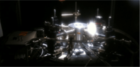
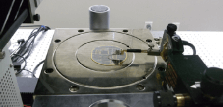
Our solar simulator is a dual source Class A close match 18 kW system, custom built by TS Space Systems. The ultraviolet and visible (UV-VIS) portion of the spectrum are created using a 6 kW mercury halide arc lamp (also known as a hydrargyrum medium-arc iodide lamp, or HMI), while infrared (IR) is produced from a 12 kW quartz tungsten halogen (QTH) lamp. The output from these lamps are individually filtered to produce either a matched AM0 (space) spectrum or, with the insertion of an additional filter set, AM1.5G (terrestrial). The system is designed to produce a 300mm diameter beam with a test plane composed of a water cooled brass chuck (10°C to 90°C). A reference cell is used to ensure temporal beam stability and numerous NASA and NREL calibration cells are available to verify close matching to AM0 or AM1.5 spectra.
Spectral Response and Quantum Efficiency
Spectral response (SR) measurements can be taken using the Newport IQE-200 Automated EQE/IQE measurement system. The illumination source can be focused to a 1mm x 2mm spot, which enables relatively high resolution spatial mapping of the spectral response from the sample when coupled with the motorized x/y stage. The system is setup with multiple detectors to measure the reference and reflected light intensity along with the current generated in the sample. This enables the measurement of both external and internal quantum efficiency through the in-situ measurement of reflection from the surface. The system is retrofitted with a Stanford Research Systems lock-in amplifier to provide very high sensitivity and a low noise floor. Multiple LED and fiber based bias light sources are available for multi-junction spectral response. Electrical bias capability is also provided using a SRS preamplifier.
Additional SR capabilities are available using an Goouch and Hosego OL-750 spectroradiometeric measurement system. This system uses low noise high precision amplification and light power supplies to provide SR measurements with low noise and high dynamic range below 10‑6 A/W. The illumination can be projecting into a Janis variable temperature micro-probe station with the ability of ranging from 4-500K to measure response as a function of temperature.
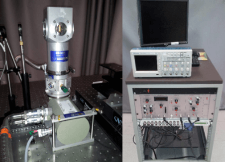
Sula Technologies Deep Level Transient Spectroscopy
Dr. Hubbard’s research group utilizes a state of the art deep level transient spectroscopy (DLTS) system that is used in conjunction with a Cryo Industries closed loop helium cryostat to probe trap states within semiconductors. Virtually all trap parameters can be determined, including density, thermal cross section, energy level and spatial profile. High sensitivity allows for detection of bulk trap densities on the order of 109 atoms/cm3. The cryostat allows temperature ranges from 10-400K, with the possibility of rapid scans up to 100K in 8 minutes. This powerful technique provides the ability to characterize the crystalline quality and defect density of the epitaxial growths that are be enabled by the MOVPE facility.
Photoluminescene, Electroluminesence and Photoreflectance
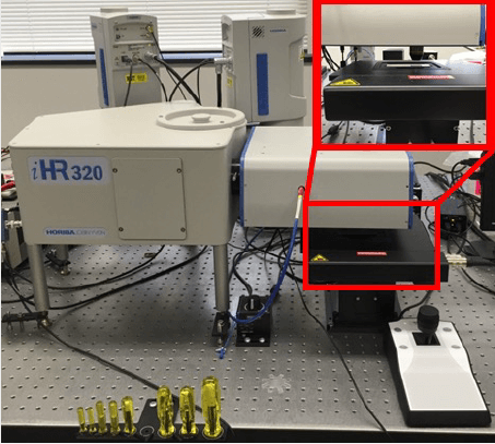
Multiple spectroscopic setups are used to characterize the material band structure, absorption characteristics and other optical metrics. Both a free space and mapping photoluminescence (PL) system are available. A Horiba iHR320 and MicOS PL mapping tool can be used for rapid and accurate characterization of photo-emission from layers and devices. Excitation is provided though a 523 nm diode pumped solid state (DPSS) laser. Detectors include a cooled Si CCD and InGaAs liner array, allowing rapid PL characterization from the deep UV to up to 1.6 microns. Wafer mapping gives information on spatial variation in intensity and wavelength across 50-100 mm wafers, essential to minimize variation and achieve consistent growth of both nanostructures and synthesized semiconductor thin films.
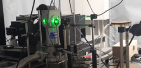
A Princeton Instruments SpectraPro monochromator allows for single point PL measurements with free-space optics with vertical sample mounting, enabling photoluminescence measurements from a Cryo Industries He recirculating cryostat (10-500K). The monochromator is fitted with a detector cradle enabling rapid swapping between detector modules, allowing for spectroscopic characterization of emission from UV wavelengths to up 4.5 µm. Excitation is provided by a 532 nm DPSS or a Spectra Physics G41 Ar-ion laser at 514.5nm.
The setup can also be modified for electroluminescence with the addition of an external bias. Both relative and absolute EL can be collected, for extraction of sub-cell Voc in multijunction devices as well as luminescent efficiency. As well, a DC light source is available for photoreflectance measurements (laser modulated reflectance), used to measure bandgap and transition energies in semiconductor thin films and nanostructures.
Electrical Measurements
Three different probe stations are available for electrical testing of devices. A dark box enclosed Cascade Microtech Manual Probing Station is coupled to an Agilent B1500 Semiconductor Parametric Analyzer for both dark I-V and C-V measurements. A Signatone probe station and customized dark box with variable intensity laps is used for JSC/VOC measurements to extract diode ideality, saturation current, shunt resistance and series resistance under illumination. Finally, a Janis variable temperature micro-probe station allows for measurement of dark IV, light IV, CV and spectral response from 4K to 500K.