Making a quantum leap
Elizabeth Lamark
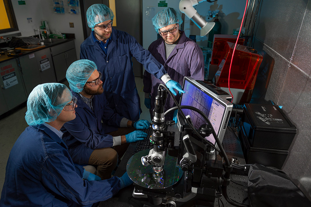
RIT researchers inspect the quantum photonics wafer under a microscope. From left to right, professor Stefan Preble; microsystems engineering Ph.D. student Matthew van Niekerk; microsystems engineering Ph.D. student Michael Fanto; and assistant professor Gregory Howland.
Researchers from RIT’s Future Photon Initiative, in collaboration with the Air Force Research Laboratory, have produced the Department of Defense’s first-ever fully integrated quantum photonics wafer.
Wafers are used to mass produce integrated circuits or microchips. The microchips produced by this wafer will help to explore how photonics can be used to develop quantum computers.
Air Force Research Laboratory: Michael Fanto and Christopher Tison
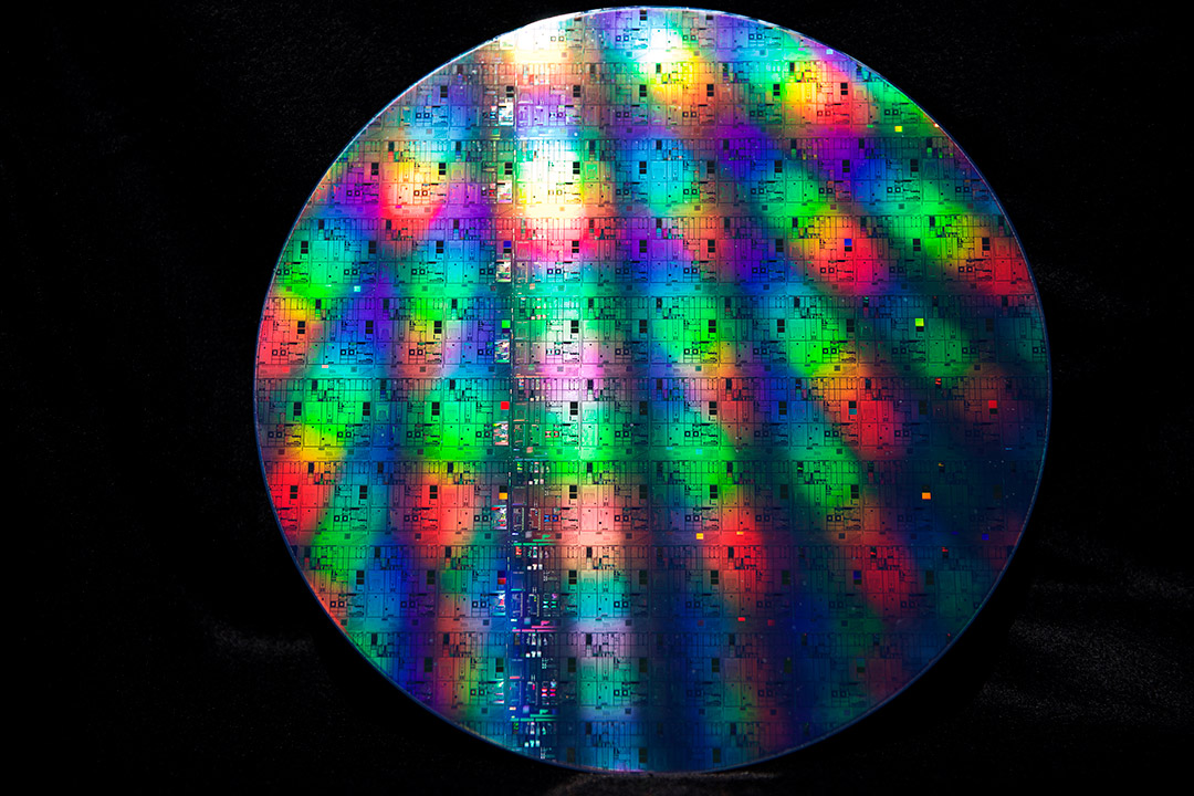
RIT researchers produced the Department of Defense’s first-ever fully integrated quantum photonics wafer, shown here. The wafer was broken into microchips to be used in quantum computing tasks.
Quantum technology leverages the effects of quantum physics at the atomic level, where different rules govern matter and classical physics is defied. Quantum phenomena such as entanglement—when particles share certain properties even when separated by an enormous distance—and superposition—when objects can be at two different states at the same time—promise to make the seemingly impossible possible.
The first wave of quantum technology included lasers, the transistor, and GPS, helping usher in the information age. Scientists have since developed a deeper understanding of the underlying quantum physics, and are now racing to develop quantum technology that would bring about a quantum 2.0 revolution and supercharge capabilities in computing, communication, imaging, and sensing.
The quantum photonics wafer project is led by the Air Force Research Laboratory and RIT. The wafer includes chip designs from both RIT and Air Force Research Laboratory, along with designs by collaborators at MIT, Purdue University, Oak Ridge National Laboratory, Army Research Laboratory, and Rensselaer Polytechnic Institute.
The wafer was fabricated by AIM Photonics in NY CREATES' advanced 300mm microelectronics facility in Albany, N.Y.
“The traditional quantum optics experiments done with single photons up until a few years ago were all realized on giant optical tables with lots of mirrors, lenses, lasers, and other bulk optics equipment,” said Stefan Preble, RIT’s lead on the project and a professor in microsystems engineering. “That’s not very scalable because it obviously takes up a lot of space,” he said. “Through this project, we are taking that giant optical table that proves these quantum concepts and miniaturizing it down onto a microchip.”
Once the 300mm wafer was created, it was divided into individual chips and the chips were distributed to the collaborators so they can begin using them in experiments to develop quantum photonics devices and circuits.
By scaling these experiments down to chips that are about one square centimeter, they can explore bigger and more complex systems.
In October 2019, Google announced it had achieved quantum supremacy, claiming it developed a quantum computer using superconducting circuits that could perform a calculation in 200 seconds that would have taken the most advanced supercomputer 10,000 years. Scientists still have a way to go before producing practical quantum computers, and photonics could be a key to achieving that.
There are several approaches to creating quantum computing devices, including using photons, trapped ions, or superconductors. But photons have an advantage over other methods because they don’t have to be cooled to extreme temperatures like superconductors or be used in a vacuum like trapped ions.
RIT researchers have been working at the intersection of photonics and quantum technology for years and last year the university brought international pioneers in the field to its first Photonics for Quantum Workshop. RIT is planning the second international Photonics for Quantum Workshop June 23-25.
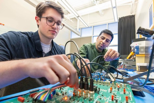
Other RIT collaborators working on the quantum photonics wafer project include Gregory Howland, an assistant professor in the School of Physics and Astronomy, and microsystems engineering Ph.D. students Matthew van Niekerk and Michael Fanto, who is also a research physicist at the Air Force Research Laboratory.
“There are a lot of important building block experiments on the wafer,” said Howland. “We’re working on making good sources of photons, circuits for manipulating them, and calibration circuits. We’re refining these individual devices and, in the future, they will be combined together to make a quantum computing device.”