Research Brief: Advanced Manufacturing
Project Brief
Type of Research: Advanced Manufacturing
Motivation for Research: The rapidly emerging Internet of Things (IoT) is driving huge demand for low cost flexible printed electronic devices. Traditional approaches to printed electronics have typically suffered from low electrical conductivity, poor adhesion to the substrate, and high cost. Until these issues are addressed, industrial adoption of low cost printed electronics techniques will be severely limited.
Research Approach
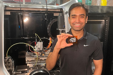
In 2017, RIT's AMPrint Center purchased the very first Vader Systems (now Xerox) metal additive manufacturing machine that jets droplets of molten metal to build up 3D parts. Professor Denis Cormier and PhD student Manoj Meda decided to see if this metal AM technique could be used to print electrical circuit patterns on flexible polymer substrates as an alternative to traditional printed electronics methods inkjet or aerosol print conductive nanoparticle inks.
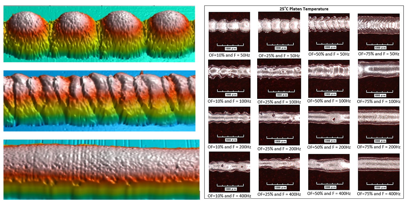
Manoj identified the key controllable process parameters, such as nozzle diameter, molten metal temperature, droplet jetting frequency, droplet spacing, and substrate heating temperature. He then conducted screening experiments followed by full-factorial experiments in which molten aluminum circuit pattern traces were jetted onto flexible polymer (polyimide) films. Through analysis of results, he found the range of process settings that simultaneously resulted in excellent electrical conductivity and adhesion of the printed traces to the flexible polymer substrate.
Manoj is complementing his experimental work with multi-physics Ansys simulations of the molten metal droplet jetting process. Through these process simulations, he is able to virtually test the results of jetting using smaller diameter nozzles, other molten metal alloys, or more temperature sensitive substrates.
Key Findings
- Unlike most nanoparticle ink printed electronics where the electrical resistivity is 2X – 10X higher than the bulk metal being used, printed electronic traces produced with molten metal droplet jetting have resistivity that matches that of the bulk metal.
- Due to the extremely high conductivity and thicker traces than are feasible to produce with other methods, very high electrical currents can be run through the printed traces without excessive heating.
- The printed circuit patterns can be flexed hundreds of times with little or no loss of electrical conductivity.
- The cost of the wire feedstock material is orders of magnitude lower than the cost of precious metal nanoparticle inks on a volumetric basis.
Looking Ahead
This work is the basis for Manoj's Ph.D. dissertation which he expects to defend in Spring 2021. He has submitted one journal paper for review, and he has two additional journal papers that are being edited for submission. Xerox has filed a patent on this work that has joint inventors from RIT and Xerox.