Short Courses

Short Courses
Electrical and Microelectronic Engineering
Short Course: IC Processing
Dates: December 15-19, 2025 and March 9-13, 2026
Cost: $1,900 per person. Discounts are given to two or more registrants from the same company. Fees cover tuition, materials, and lab fees. RIT reserves the right to cancel a given offering if enrollment is too low.
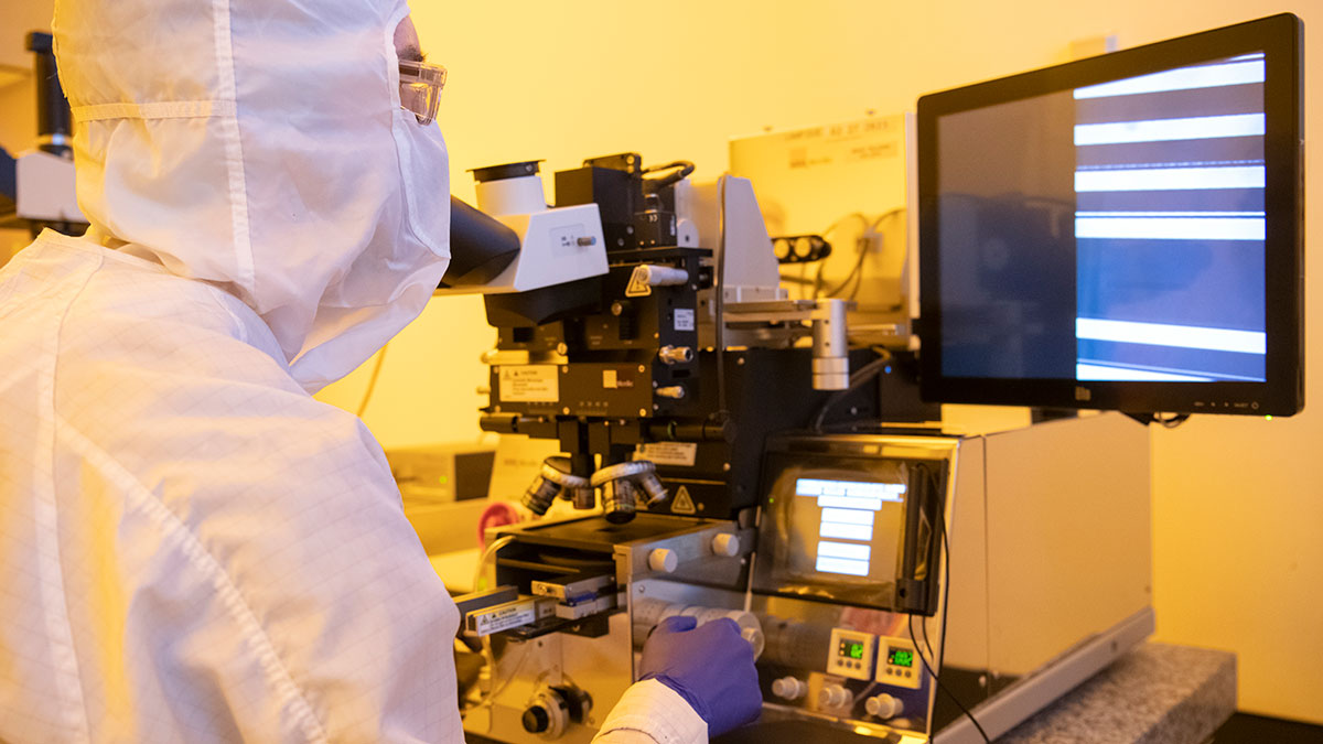
Objective: This course provides a comprehensive, hands-on educational experience in integrated circuit process engineering through a combination of lectures and cleanroom based laboratories. Participants not only learn about semiconductor device structures and the processing steps to fabricate them, but are also exposed to CAD layout, mask making basics, IC testing, and SPC methodology as well. A four-level metal gate PMOS process is used to fabricate the student designs on 150mm Si wafers using i-line stepper lithography.
Who Should Attend: This course is intended for individuals seeking a better understanding of the overall theory and practice of microelectronic engineering, and an appreciation of how the processing steps interact. Ideal applicants may be individuals trained in one specific aspect of IC processing such as chemistry, physics, or electrical engineering, newly hired to the field, or looking to make a career move.
More than 1000 people have completed this course since it was first offered in 1986. They were process engineers or technicians, managers, sales reps, educators, scientists, and graduate students from both foreign and domestic institutions.
Participants will be designing a basic device on Mentor Graphic tools complemented by Silvaco Process Simulation Software. Chip fabrication occurs in a 10,000 sq Ft., class 1000 cleanroom housing more than $20M worth of IC processing equipment including oxidation and diffusion furnaces, an ion implanter, CVD systems, both i-line and g-line steppers for lithography, sputter tools, wet and dry etch equipment, and in-process metrology tools. An IBM AS/400 computer tracking program is used for work-in-progress tracking.
The course runs M – Th (8 am – 5 pm) with an hour break for lunch, and F (8 am – 3 pm) with an hour break for lunch.
Day 1: Overview of IC processes and the corresponding device physics, followed by the basics of IC CAD and the layout lab.
Day 2: Lecture on the PMOS process flow, along with lecture and lab on cleaning, oxidation, and lithography of level 1.
Day 3: Semiconductor doping lecture and lab, along with lectures on CVD and dry etch. Second level lithography and overlay are completed.
Day 4: Lab involves gate oxide growth and third-level lithography for contact cuts, while lectures cover advanced CMOS, metallization, and CMP. Al- sputter coating begins.
Day 5: Completion of metallization and 4th level lithography so wafers are ready to test in the afternoon. Lectures on device simulation, SPC, and case studies on yield issues occur in the
morning.
I just want to say thank you again for everything. I am sitting here flipping through my binder reviewing everything I learned all week. I feel very privileged to have spent an entire week with a team of professionals that so enthusiastically shared their knowledge and experiences with me. I learned a lot. Please tell everyone from grad students, doctors and tour guides thank you from the bottom of my heart! Everyone had their unique style of presenting which helped me put two and two together. I am looking into taking an online class to continue my education. And, my husband is so impressed with everything he's taking the tape of resistors to work for show and tell! I feel so lucky and grateful for being able to take advantage of this opportunity.
- Archive Administrator with Semiconductor Manufacturer
I wanted to take the opportunity to thank you for the great training that was provided last week. I learned a lot about Integrated Circuit fabrication that I did not know before. The mix of classroom learning and the hands-on labs were just right. The instructors were excellent and the support from the grad students in the lab was very good as well. The course content gave a good and complete overview of modern semiconductor manufacturing techniques. I understand that it’s hard for a university or research facility to keep up with state of the art equipment, so I really enjoyed Dr. Hirschman’s lecture on Advanced MOS Processing. A great big thank you to Dr. Jackson, Dr. Fuller, Dr. Hirschman, Dr. Pearson, Dr. Kurinec and Ms. Bolster!
- Test Engineering Manager with Aerospace and Defense Company


