Center for Electronics Manufacturing and Assembly supports educational and workforce development initiatives
Center for Electronics Manufacturing and Assembly supports educational and workforce development initiatives
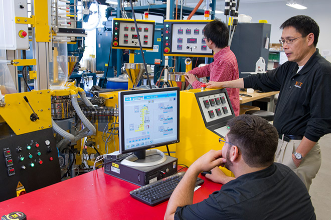
The College of Engineering Technology’s Center for Electronics Manufacturing and Assembly (CEMA) was established at RIT in 1995 and provides workforce training, development, prototype testing, and research for the electronics manufacturing and packaging industry. CEMA supports local companies in building test beds for prototype electronics devices that are exposed to different types of electrical, optical, or thermo-mechanical stresses to test reliability and functionality. Work in CEMA will also contribute to the growing photonics industry, expected to have a multi-million dollar impact on today’s economy.
“The American Institute for Manufacturing Integrated photonics organization (AIM Photonics) has plans to do those same types of tests for new integrated photonic circuits, but that is further downstream, and they have more immediate needs right now,” said Martin Anselm, faculty-researcher and director of CEMA.
Attaching fiber optics to the circuit is a complex and time-consuming part of the process, even before the chips can be mass-produced for devices. Researchers such as Anselm are working on both fiber attachment solutions and related manufacturing processes.
Fiber must align on the silicon, but it is much smaller than components for an electronic circuit, needing precision and different materials to anchor the fiber to the base chip.
With an electronic circuit, electrons pass through a conductor such as copper or the soldering material. Heating to its melting point, that material coalesces into separate, tiny droplets that align with features on the circuit board to close the electrical circuit. This was described by Anselm as an overall process challenge.
For photonics, light in an optical fiber needs to be perfectly aligned to a feature on a piece of silicon. Light is sent through the fiber, and a reading of its peak intensity is measured.
“Now the challenge becomes how am I going to hold that fiber in place? Researchers are trying to apply electronic circuit attachment concepts to photonics but there is no solution—yet,” said Anselm, who added that fibers must be affixed with materials that do not degrade due to heat or humidity inherent in the close proximity of the circuit’s structures and interfaces. Further manipulation of the circuit is needed to protect the fiber before testing.
AIM Photonics was created to build streamlined high-volume, manufacturing capabilities. That infrastructure doesn’t exist today because the technology to build photonic devices is so sophisticated that only the most elite companies can do it, and usually for only specialized applications such as military heads-up displays, Anselm explained. Utilizing the model of the electronics industry infrastructure, fine-tuning it, and making it more precise is a goal, but comes with a downside. The current outcome is a slower process with higher costs, impacting volume.
“If you do things one or two-at-a-time, and it takes an army of Ph.D. engineers to put something together, then the price is astronomical,” said Anselm, who will provide photonic packaging education materials that will be used for all levels of training needs. “But, part of the long-term, broader impacts to all this type of research and work that AIM Photonics is doing—that RIT is doing—is to try to develop the technology that will make it more mass producible.”