Innovation in Microelectronics
The development of integrated circuits and semiconductor devices has revolutionized our society from communication to information storage to transportation and media. The creation and implementation of a wide variety of digital devices central to our daily lives would not be possible without these technologies. Given the continued demand for micro and now nano electronics, researchers are working to further enhance the speed and storage capacity of these next-generation devices.
A Leading Innovator
“By increasing the functionality of micro and nano electronics, we can improve quality and performance while opening up new avenues for microelectronics applications,” notes Santosh Kurinec, head of the department of micro-electronic engin-eering at Rochester Institute of Technology. “These efforts will ultimately have major implications for a wide range of disciplines including medicine, transportation, entertainment, and energy management.”
These innovations require new devices, novel materials, and innovative fabrication methods to accomplish improvements in microelectronics as well as more skilled engineers and researchers to make it happen. There are very few academic institutions that have a stronger background and skill set in this area than RIT. The university was the first in the nation to create a department devoted to microelectronic engineering, which celebrated its 25th anniversary in 2007, and also the first to create a doctoral program in micro-systems engineering. Research conducted at RIT has advanced numerous tech-nologies, including quantum devices, nanolithography, and nanomaterials. In addition, graduates of the program are now employed by nearly every major semiconductor company working in the field, including Intel, IBM, and Micron. “RIT has a long history of success in micro and nano electronic education and research, and has made a major contribution to the field’s development over the last quarter century,” adds Kurinec. “Our current efforts build on our commitment to grooming researchers for the ever-evolving microelectronics industry.”
Professor Kurinec’s team is adding to this body of research through groundbreaking work in the area of silicon integration. This effort focuses on looking for new methods to integrate disparate materials onto traditional silicon chips, enhancing functionality, memory, and speed. These have included luminescent phosphors, high-permeability magnetic cores, and spin-based junctions. To pursue these initiatives Kurinec has partnered with Surendra Gupta, professor of mechanical engineering, in establishing a state-of-the-art nanocharacterization facility that includes a Bruker D8 Discover High-Resolution X-Ray Diffractometer and a Multimode Atomic Force Microscope. Currently, Kurinec and collaborator Sean Rommel, associate professor of microelectronic engineering, are working to monolithically integrate silicon nanoelectronics with charge- and spin-based tunnel devices.
Spintronics and Next-generation Microelectronics
Spintronics, or magnetoelectronics, utilizes ferromagnetic materials—compounds with an inherent magnetic behavior—to capture the spin state of the electrons. The process is now used in the development of mass storage devices and magnetic random access memory (MRAM), which utilize spintronics to greatly enhance the amount of data that can be stored. Scientists are now testing devices that can compress data down to one trillion bits per square inch. Eventually, researchers hope to use the method to create spin-based transistors powered by magnetic semi-conductors that require little external energy and greatly improve memory capacity over traditional devices.
Kurinec and Rommel are working with Veeco Corporation and the Naval Research Laboratory to integrate magnetic tunnel junctions, a spintronics device, with resonant tunnel diodes, which utilize the quantum effect generated by different compound semiconductors to create an electromagnetic wave that can be used in high-speed circuitry. The combination of the two technologies in a traditional Complementary Metal–Oxide–Semiconductor (CMOS) integrated circuit could greatly increase the tunneling magneto-resistance ratio, which is used to measure how effectively the magnetic charge is being transferred. Kurinec and Rommel believe the technique can increase the quality and reduce the costs associated with the process and ultimately enhance the utilization of spintronics methods, such as MRAM, for use as storage methods for electronic devices.
“Currently, MRAM chip technologies require a relatively larger amount of energy to operate, which increases the cost and reduces the effectiveness of these devices for smaller, low-power applications,” says Rommel. “Through the combination of magnetic tunnel junctions and resonant tunnel diodes on a CMOS circuit, we hope to increase the efficiency of the process and expand the uses for MRAM in a host of areas.” Kurinec and Rommel’s work in the field builds on more than a decade of research conducted by Kurinec’s team, which has made major strides in the implementation of additional semiconductor materials besides silicon, for use in transistors and integrated circuits.
For example, in 2000 Kurinec partnered with the Ohio State University to integrate silicon-germanium-based semiconductors, using the technique known as MBE (molecular beam epitaxy), onto CMOS-integrated circuits. This was the first time that MBE grown semiconductors had been successfully incorporated into a CMOS device, and the data and knowledge the team developed on the project led to their interest in integrating magnetic tunnel junctions with CMOS circuits.
“The previous successes we have had in materials integration serve as building blocks for our current and future research efforts,” states Kurinec. “The diversity of materials and techniques we have worked in allows the team to apply our knowledge to a wide variety of applications within the integration arena. This environment not only increases the quality of our work but also further promotes RIT’s micro-electronics capabilities for research with government, academia, and industry.”
Kurinec’s current major research effort grew out of a senior undergraduate project leading to a master of science thesis by Michael Latham involving fabricating devices on strained silicon wafers donated by AmberWave Systems. Subsequently, Kurinec, Rommel, and fellow microelectronic engineering faculty member Karl Hirschman partnered with AmberWave to receive NSF funding for integrating III-V materials onto silicon-based devices.
III-V materials, so named because of their location on the Periodic Table, have been used for years in niche markets that require extreme high-speed performance, optical properties, and/or radio frequency properties. However, they have seen little market penetration for more mainstream applications due to high costs and difficulty in integration with conventional, inexpensive silicon electronics.
This new research partnership will seek to develop the use of Aspect Ratio Trapping, or ART, an innovation created by AmberWave Systems to enhance the use of III-V materials in a number of applications. The team will test the quality of the process and work to develop a prototype manu-facturable system incorporating III-V and silicon devices together.
“The joint venture between RIT and AmberWave is an example of our interest in cultivating technology from the ground level up,” notes Richard Faubert, president and CEO of AmberWave. “We are extremely enthusiastic about what the partner-ship will bring to the advancement of semiconductor devices.”
Two Goals: Innovation and Educational Excellence
The partnership with AmberWave Systems, like all of Kurinec’s projects, will also include significant student involvement, including undergraduate and graduate researchers. This training component exemplifies the hands-on, educational approach that complements the micro-electronic engineering department’s research efforts. Kurinec believes this process not only benefits RIT’s students but also provides future employers with engineers who already have significant real-world experience prior to joining the workforce. A doctoral student who assisted with the Ohio State project in 2000 was ultimately hired by Intel to carry out Intel’s semiconductor research and development.
“Throughout my time at RIT I have focused on the dual goals of advancing technology in the microelectronics field, while also promoting the skills and capabilities of our students,” says Kurinec. “We believe strongly in experiential learning and feel our extensive inclusion of undergraduate, master’s degree, and Ph.D. students in our research efforts enhances our education initiatives while ultimately creating better engineers.” This innovative educational approach in microelectronics has earned Kurinec’s team a major National Science Foundation award for Leading Microelectronic Education to New Horizons.
“The ability to take my classroom training and apply it to real-world problems while I am still in school will be invaluable in enhancing my skill set and increasing my future employability,” adds Raymond Krom, an RIT microelectronics student who will be working on the AmberWave project. “It also is incredibly gratifying to be working on cutting-edge technology that will ultimately lead to new innovations in the field.”
Krom also was recently selected for an International Research and Education Experience (IREE) award from the National Science Foundation, which is allowing him to spend six months as a student researcher with IMEC, a university-industry research consortium based in Brussels, Belgium.
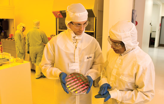
It is a testament to RIT’s ability to meet the dual goals of innovation and education that many past graduates have returned to the school as professors and researchers. Karl Hirschman, who received a bachelor’s degree in microelectronic engineering from RIT and subsequently received his Ph.D. in electrical and computer engineering from the University of Rochester, now serves as an associate professor in the departmentas well as director of the Semiconductor and Microsystems Fabrication Laboratory (SMFL)—RIT’s 13,000-square-foot clean room.
“RIT’s focus on ‘education by doing’ is a major asset not only for students but also for professors and researchers,” Hirschman notes. “Students bring new ideas and a fresh perspective to problems that assist in making our research better.”