Student awarded scholarship for circuit board work
Andrew Daya recognized for research in package-on-package technology for circuit board assembly
Michelle Cometa
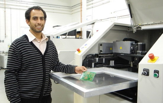
Andrew Daya, a graduate student and research assistant in the Center for Electronic Manufacturing and Assembly, explains the process of integrating electronic components onto printed circuit boards.
Printed circuit boards for consumer electronics are like a city skyline. With limited real estate to build across a neighborhood block, developers build up, story-upon-story. Memory chips and logic devices are being stacked in a similar fashion on circuit boards the size of credit cards as a way to increase power and performance across the board’s “real estate.”
Andrew Daya, a graduate student at Rochester Institute of Technology, is researching improvements to package-on-package technology—the method used to 3D-stack components on printed circuit boards—and was recently awarded the 2013 Charles Hutchins Educational grant from the Surface Mount Technology Association. It was the first time an RIT student received the award.
The $5,000 scholarship grant is given to a university graduate student pursuing an advanced degree in electronics assembly, packaging or related field, and participating in research or a project that furthers the electronics manufacturing industry. Daya was awarded the grant for his research, detailed in his paper, “Package-on-Package: A comprehensive study of the profile requirements, alloy combinations, location influence and reliability performance.” He’ll present the work at the association’s conference Oct. 13-17 in Ft. Worth, Texas.
“Instead of having a separate memory chip or separate video card, for example, and having them take up two different footprints on a circuit board, you stack them vertically,” says Daya who is in the mechanical and manufacturing systems integration graduate program in RIT’s College of Applied Science and Technology. “This is three-dimensional stacking basically, and that takes up only one footprint instead of two.”
Current electronic device manufacturers are required to transition from using lead-based alloys on circuit boards, and companies are exploring use of alternative materials to solder components on the boards. Daya’s research focuses on improving the process to design and integrate package-on-package components and on testing the reliability of several types of non-lead alloys used as part of the soldering process to attach components to the printed circuit boards.
The market for more powerful electronic devices has increased. Devices such as smart phones, video gaming consoles and computer systems have become smaller. The stacking technology allows for an increased number of components on the board, better connections between the electronics and increased reliability of the devices, Daya says.
Package-on-package technology is becoming more prominent, but due to restrictions in use of hazardous substances, researchers are testing both the reliability of the new technology and learning, at the same time, of the reliability of lead-free solder. Daya oversees reliability testing of the non-lead alloys and preparing for testing thermal shock influence on the devices.
The work is being done in RIT’s Center for Electronics Manufacturing and Assembly, a multipurpose academic facility used by students and faculty for design projects, industry research and development and corporate training, says Manian Ramkumar, director of the center and department head of RIT’s mechanical and manufacturing engineering technology program.
”Over the past decade, CEMA has established a strong presence in the electronics packaging industry for its workforce training and applied research prowess, which we are extremely proud of,” says Ramkumar. “We can attribute this to the intellectual contributions and dedication of graduate students such as Andrew.”
Both Ramkumar and Daya believe the technology is advancing, and package-on-package arrays will become more prevalent in the manufacturing industry, and may be a means to influence its resurgence in the U.S.
“Manufacturing in America is no longer an assembly worker,” says Daya, who is from Franklin, Mass. “We need engineers and people trained to control automation, to run the statistical analysis. This research will give the industry information about whether package-on-package is a good use for their applications. It will be information they need to make the right design, assembly and manufacturing choices for their products.”
Recommended News
-
April 25, 2024
!['Students are shown gathering around a snowmobile, which is one of the exhibits at Imagine RIT.']()
Imagine RIT returns Saturday with over 400 student exhibits
WHEC-TV showcases Imagine RIT, spotlighting diverse exhibits from neurotechnology and virtual reality to glass blowing and astronomy. -
April 25, 2024
![I voted sticker and checkmark.]()
Informed voting in the age of Artificial Intelligence
Artificial intelligence (AI) has entered the election—globally. To help voters navigate these advancements in social media, deepfakes, manipulated images, and cybersecurity, a few RIT experts are weighing in.
-
April 25, 2024
!['a group of staff members in yellow shirts gather under a tent being used as an information booth.']()
Staff volunteers make Imagine RIT shine
RIT staff members volunteer at the festival to assist the university in creating an unforgettable event each year by handing out welcome bags, supervising parking lots, and showing campus visitors around the bustling campus, among other duties. More than 200 staff volunteers annually commit their time to Imagine RIT.
-
April 24, 2024
![David Munson, Jr., RIT President, stands on the second floor balcony of the SHED holding a portrait that shows the renderings before it was built.]()
RIT President David Munson to step down in 2025
Spectrum News features David Munson's retirement plans for 2025, emphasizing his impact on RIT's growth in enrollment, research funding, and global presence.


