Microsystems Engineering Ph.D.
Department of
Microsystems Engineering Ph.D.
- RIT/
- College of Engineering/
- Academics/
- Departments/
- Microsystems Engineering Ph.D.
Contact
Overview
The Kate Gleason College of Engineering’s doctorate degree in microsystems engineering is a multidisciplinary program that builds upon the fundamentals of traditional engineering and science, combined with curriculum and research activities addressing the numerous technical challenges of micro- and nano-systems. These include the manipulation of electrical, photonic, optical, mechanical, chemical, and biological functionality to process, sense, and interface with the world at a nanometer scale. The goal of the program is to provide a foundation for microsystems engineers to explore future technology through research in nano-engineering, design methods, and technologies for micro- and nano-scaled systems.
Some of the program’s areas of exploration include:
- Next-generation nanoelectronics including:
- development of new techniques, processes and architectures for nanoelectronic and nano-optoelectronic devices
- exploration into new materials research including germanium, III-V materials, carbon annotubes, and spintronics
- Photovoltaic research in silicon, compound semiconductor, and organic solar cells
- Photonics and nanophotonics imaging, communications, and sensing research including couplers, micro-lasers, microdetectors, integrated silicon waveguides, silicon spectrometers, and biosensors
- MEMS (micro-electro-mechanical systems). MEOMS (micro-electro-optical-mechanical systems), and NEMS (nano-electro-mechanical systems) device, processing, and materials research for smart sensors, actuators, biochips, and micro-implantable appliances
- Scaled micro- and nano- electronics for integration into biomedical systems
- New and improved technologies in organic electronic components and devices
- Nanomaterials research including carbon nanotubes, nanoparticles, quantum dots, self-assembly materials and their applications in electronics, optics, and materials science
- Microfluidics research on the behavior, control, and manipulation of fluids at the micro-scale
The microsystems engineering doctorate requires concentration and specialization in an associated research area as well as mastery over the fundamentals of microsystems engineering. The degree is awarded in recognition of demonstrated proficiency and high achievement in the student’s concentration within the program. A significant contribution to the knowledge in the area of microsystems engineering is made through successful dissertation research and publication. The program curriculum has been designed to meet the individual needs of graduate students while ensuring that all students complete a well-rounded program of study.
A total of 66 semester credit hours of combined graduate course work and research are required for completion of the program. The course work requires a combination of foundation courses, major and minor technical area courses, and electives. The student must pass the Qualifying Exam, the Candidacy Exam, and the Dissertation Defense Exam for completion of degree requirements. Additional curriculum details can be found in the Microsystems Engineering Ph.D. Graduate Student Manual.
Research
Microsystems engineering builds on the fundamentals of traditional engineering and science to process, sense, and interface with the world at the micro- and nano- scales. Innovative research programs span across fields of biomedical, electronic, photonic, mechanical, materials, and computing engineering and sciences. Research opportunities span multiple areas of expertise, including:
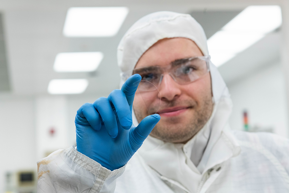
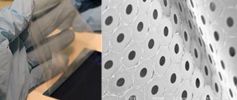 The research and fabrication of nanomaterials promises to revolutionize a number of industries and scientific fields, particularly biomedical devices and stem cell engineering. A major barrier to significant adoption and incorporation of novel nanomaterials is the need to produce these materials in high volume and at low-cost. We research the fabrication of ultrathin nanomembranes and the methods to produce these materials more simply, while retaining their unique properties. Additionally, we use these nanomembranes to create tightly controlled cellular microenvironments for adult stem cells. These microenvironments are used to help study and induce the differentiation of stem cells for potential uses in tissue engineering. Specifically, we are investigating the differentiation of adult adipose-derived stem cells into cells that can create and support the development of vascular networks. Scale-up of these methodologies for future use in tissue engineering will require high volume production of nanomaterials as the differentiation substrate.
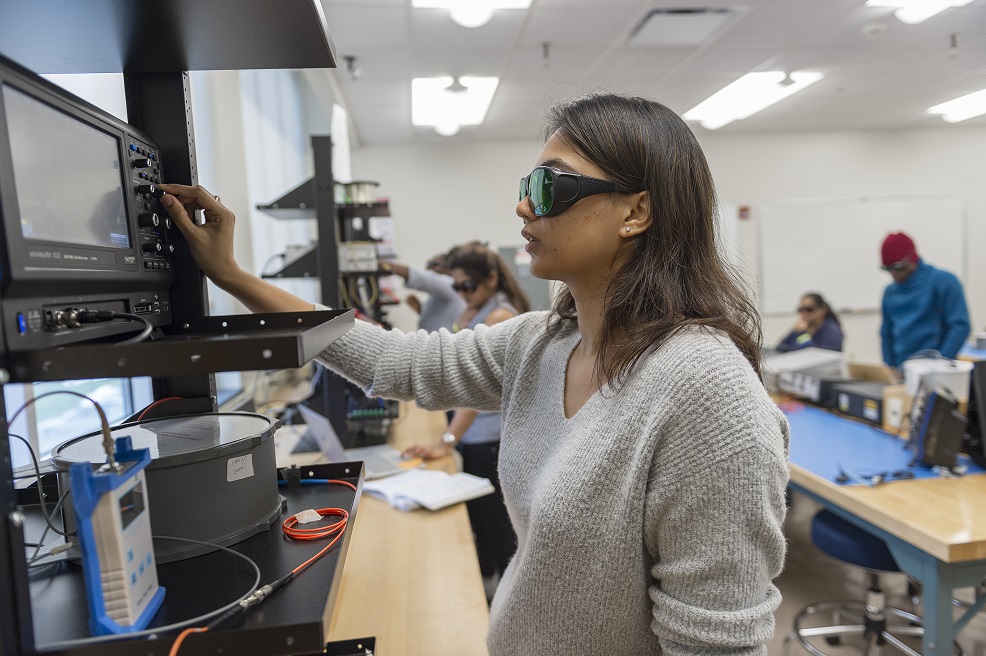
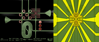 The Nanophotonics Group is developing silicon photonic chips that will revolutionize computing, communication, and sensing systems. Silicon enabled the electronics age with its good electrical properties, high purity, and scalable manufacturability. However, all electronic devices face imposing performance and energy challenges due to the fundamental limits of electrons. In contrast, photons propagate at the speed of light, can carry vast amounts of information (10’s of Tbit/s), and have minimal noise. By using the same Silicon nanofabrication manufacturing technology used to make all integrated circuits, the RIT Nanophotonics group is realizing Silicon nanophotonic devices and systems that have high performance and the potential for low cost. The groups research is focused on several key areas: optical interconnects for chip-to-chip and on-chip low energy communications (lasers, electro-optic modulators, multiplexing techniques); Silicon compatible nonlinear optics (amorphous Silicon, Silicon nanocrystals); quantum optical computing and communication (photon sources, gates, and detectors); and ultra-sensitive optical sensing. The research has been supported with funding and close collaborations with a wide range of government and commercial entities.
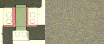 The research activities in the Thin Film Electronics group are focused on inorganic thin-film electronics on both silicon and non-silicon platforms. Research on low-temperature polycrystalline silicon (LTPS) is exploring an alternative method of crystallization using a flash-lamp annealing (FLA) process. The instrument uses Xenon flash-lamps with an extremely high irradiance to expose samples with pulses in the microsecond timescale, and was acquired by Prof. Denis Cormier in the Industrial & Systems Engineering Department at RIT. We have most recently demonstrated the ability to form large-grain material with domains that appear to be 10’s of microns in size; the electronic quality of the material is still under investigation. Thin-film transistors (TFTs) made at RIT using sputter-deposited Indium-Gallium-Zinc-Oxide (IGZO) demonstrate results among the best reported in the literature, with continued efforts focusing on passivation materials for improved device stability and process integration. Even though there has been limited introduction of IGZO TFTs in display products, this work continues to be relevant and of significant interest to the display industry. Other metal-oxide semiconductors as well as two-dimensional materials (e.g. MoS2) are of interest for VLSI in addition to applications on alternative substrate materials.
Professor Seth Hubbard
Physics / Microsystems Engineering
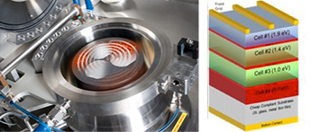 The conversion of light from the sun into electrical energy is playing a very important role in our current challenge for alternative energy technologies, to reduce our dependence on fossil fuels as well as reduce greenhouse gas emissions. The vision of Dr. Hubbard’s research group is to accelerate scientific breakthroughs in the discovery of materials and structures that will advance the frontier of the conversion of light to electricity. The group’s focus is on new material systems, fabricating them, and demonstrating proof-of-principle of devices that will deliver a major boost to the world’s pursuit of innovative and transformative energy conversion products. Their strategy to make this outcome possible is through nanoscale and/or novel material (a) synthesis, (b) modeling, (c) characterization, and (d) fabrication of energy conversion devices. The team’s expertise lies in vapor phase epitaxy (VPE) of III-V photovoltaic devices and nanostructures, novel photovoltaic structures such as the intermediate band solar cell, photovoltaic characterization as well as simulation and testing. The outcome of their work could advance (1) the state-of-the-art in device efficiency and (2) lower cost for the conversion of light to electrical energy.
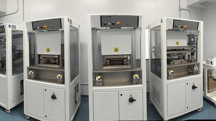
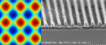 Nanofabrication technology has been central to the field of semiconductor device manufacturing for many years. As applications grow beyond microelectronics, new needs for research into nanoscale patterning and materials emerge. The Nanolithography Research Laboratories at RIT has pioneered key advances in nanopatterning and materials technologies that have driven nanolithography into sub-30nm regimes. Activities are underway in optical (UV, VUV) and EUV lithography as well as non-conventional nanopatterning techniques and materials for new applications in micro and nanoelectronics, plasmonic structures, organic electronic devices, micromechanical and microfluidic MEMS and NEMS, bioNEMS, patterned magnetic media, and liquid crystal displays. Research is being carried out for the extension of far-field projection lithography, high index immersion lithography, near-field lithography, polymer systems, thin film materials, and sub-diffraction plasmonic imaging. Faculty and students are actively involved with collaborative research with partners in the US, Europe and Asia with support from industrial and government funding organizations.
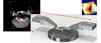 Investigating and modelling the mechanical properties of materials is important for many applications. The most common technique used for mechanical characterization of materials is called nanoindentation. The currently available tools utilized in order to perform nanoindentation have their limitations in terms of sensitivities of force and displacement or limitations due to the hardware for a broad range of material properties. When it comes to investigation of soft materials, these limitations might be more detrimental. In Multi Agent Bio Robotics Laboratory (MABL), we have been working on development of novel nanoindentation techniques with a multi-probe atomic force microcopy (AFM) system in order to ease the major problems encountered with standard AFM or nanoindentation systems. Tuning forks are used as probes during nanoindentation. For quasi-static nanoindentation experiments, our approach extracts the force information through the displacement of the indenter probe measured by a second probe with ultra-resolution. For dynamic nanoindentation techniques, a single probe frequency modulation of the indenter tuning fork is used to extract force information. Thanks to the high quality of resonance (Q factor) of tuning fork probes, force measurements can be performed with a resolution as small as 1.6 pN. The accurate measurements of material properties on soft materials is used in characterization of microfabricated pillar sensors which can be used in measuring forces on cancer cells for observing cell traction. The technique developed in this research also enables us to use the system as ultra-sensitive force sensor to apply nN scale lateral and vertical loads on microfabricated structures or biological specimens.
Recently the Rochester Institute of Technology has demonstrated the co-integration of CMOS devices and resonant interband tunnel diodes (RITDs). Our strategy has been to integrate the tunnel diodes following all high temperature steps, but prior to the contact metallization of the CMOS devices. A recent paper in the Sept. 2003 issue of IEEE Transactions on Electron Devices co-written by our sister group at the Ohio State University found that compared to the performance of bulk RITDs used as a control (with a peak-to-valley current ratio or PVCR of 3.8), the integrated devices exhibited a slight degradation performance (PVCR of 3.4). We have also published a paper at the University-Government Industry Microelectronics Conference (UGIM 2003) that showed a slight reduction in performance for integrating atop implant regions. When formally integrated atop CMOS, the PVCR ultimately was found to be 2.8. Details of this work were presented in Washington, DC at the 2003 ISDRS conference. We also have recently demonstrated a simple latch-based circuit in the form of a MOnostable BIstable Logic Element (MOBILE) incorporating an integrated FET and RITD. We believe that the MOBILE serves as a proof of concept, providing a roadmap as to the biasing conditions where the tunnel diode will ultimately be useful with CMOS.
![]() The Semiconductor Photonics and Electronics Group focuses on developing highly efficient III-V and III-Nitride semiconductors for photonic, optoelectronic, and electronic devices. High-efficiency III-V and III-Nitride semiconductor based photonic and optoelectronic devices such as lasers and light-emitting diodes (LEDs) are considered as promising candidates for next generation communication and illumination system. The research group is working on the development of novel quantum well active regions and substrates for enabling high performance ultraviolet and visible LEDs/ lasers, as well as the engineering of advanced device concept (surface plasmon and nanostructure engineering) for high-performance nanoscale photonic devices through the study of strong light-matter interaction. The group is also developing novel III-Nitride materials for next-generation analog electronics which would be compatible with the existing Si technology.
The Semiconductor Photonics and Electronics Group focuses on developing highly efficient III-V and III-Nitride semiconductors for photonic, optoelectronic, and electronic devices. High-efficiency III-V and III-Nitride semiconductor based photonic and optoelectronic devices such as lasers and light-emitting diodes (LEDs) are considered as promising candidates for next generation communication and illumination system. The research group is working on the development of novel quantum well active regions and substrates for enabling high performance ultraviolet and visible LEDs/ lasers, as well as the engineering of advanced device concept (surface plasmon and nanostructure engineering) for high-performance nanoscale photonic devices through the study of strong light-matter interaction. The group is also developing novel III-Nitride materials for next-generation analog electronics which would be compatible with the existing Si technology.
Professor Mishkat Bhattacharya
Physics and Astronomy
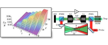 Our group is broadly interested in light-matter interactions from the perspective of fundamental science as well as technological applications. Currently we are focused on the interplay of electromagnetic modes of radiation, such as laser light, with nanofabricated components, such as mechanical oscillators and rotors. Our aims are the cooling of macroscopic objects into the quantum regime and to establish the limits to quantum sensing of mechanical displacement, force, and rotation, for example. These investigations are expected to test the foundation of quantum mechanics as well as to yield next generation sensors that circumvent the limits posed by quantum mechanics to their sensitivity. Some of our effort also goes towards investigating other related platforms for quantum technologies such as ultracold atoms and molecules. Our work is fully theoretical, involving mostly analytical calculations, using the techniques of quantum optics and atomic physics, and some medium-scale numerical work. We collaborate closely with experimental groups locally, nationally, as well as internationally. Our program involves researchers at every level, including undergraduate, masters, and doctoral students as well as postdoctoral scholars. Recent funding sources include the Research Corporation for Science Advancement, the Office of Naval Research, and the National Science Foundation.
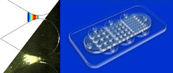 The Microsale BioSeparations (MBS) Lab is a research group working on separation, sorting and detection techniques of nano and microbioparticles, such as macromolecules and cells. We employ electric field driven techniques (dielectroforesis, electrophoresis and electroosmosis) in microfluidic devices. This is a very multidisciplinary area that combines microfluidics, electric fields, chemistry and biology. Our main objective is to develop robust and rapid microfluidic-based techniques to offer an alternative to traditional bench scale analytic/separation/purification processes. Our ultimate goal is to contribute the field of lab on a chip, aiming to create portable laboratories. We work with a wide array of bioparticles, from proteins and DNA to virus and many types of bacterial and yeast cells. Our projects involve both, experimental work and mathematical modeling (with COMSOL), we are currently working on several projects focusing on the manipulation of microparticles and cells with low frequency AC electric fields and on the understanding of the forces that generate dielectrophoretic capture of microparticles in microdevices. Our research efforts have been supported by NSF.
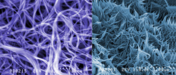 The group’s research activities focus on enhancing the performance of energy conversion, transmission, and storage devices through the use of nanomaterials. Current interests include the development of high capacity anode and cathode active materials for lithium ion batteries as well as engineering novel device architectures using carbon nanotubes (CNTs). A second research area focuses on fabricating and improving the electrical conductivity of bulk CNT wires and cables for power and data transmission. In addition, fundamental studies on CNT synthesis, electronic type separations, thermal and chemical stability, and material tolerance to harsh radiation environments are being pursued. As the group’s leader, Dr. Landi maintains a robust and mature research program which includes a diverse group encompassing postdoctoral fellows, multiple full-time research staff, PhD students in sustainability and Microsystems engineering, and various undergraduate researchers across engineering disciplines.
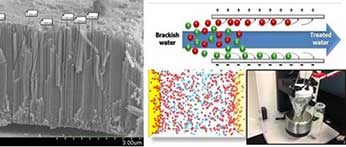 Innovative and greener chemical processes are needed in order to address societal grand challenges, which mostly involve conservation of resources. One of such societal grand challenges is future fresh water supply, for example. New water desalination technologies are urgent considering that 98% of water available in our planet is sea water or brackish water. Our research group focuses on the development of next generation chemical processes to address this kind of challenges that are energy-efficient, low-waste, and with low installation and maintenance costs. We identify physicochemical and transport mechanisms specific to different chemical species that can be triggered by carefully designing separation media and operation conditions. Therefore, we start with basic research on phenomena at the molecular scale that we can exploit and potentiate to develop a chemical process. And, then, we move into applied research of materials and operations in order to devise the chemical process per se. Our methods include a combination of experiments and modeling from the molecular to the macro-scale. Current projects include the development of a family of processes driven by the application of low-voltage electric fields for the purposes of water desalination, selective water deionization, advanced waste-water treatment and electrocatalysis. We are also working in a family of processes for the application of gas hydrates in gas storage and transportation, as well as gas separations.
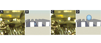 The Thermal Analysis, Microfluidics and Fuel Cell Laboratory (TAmFL) at RIT has gained international recognition for advances in fundamental research. With nearly two dozen student researchers, the laboratory immerses students in real-world research that establishes students within the industry long before graduation. Nearly 20 years ago, the laboratory was founded to focus on understanding the fundamentals of microfluidics and the phenomena of heat transfer. The research conducted is driven by actual industry challenges that allow students to learn at a level that will enable them to be innovators and influence future technologies. The lab's early research focused on microscale fluid mechanics and heat transfer and positioned it as an international leader. Today, the lab has expanded to encompass a range of microfluidic applications, including pool boiling, heat transfer on a silicon chip, and water management of proton exchange membrane (PEM) fuel cells. Students are the centerpiece of the research at TAμFL. It is amazing to witness the dramatic transformation as students unravel a new dimension of their talent and are contributing at the cutting edge of the technology. They are on their way to become the top researchers in their chosen field with an unparalleled combination of fundamental and applied science perspective.
Professor Chris Collison
Chemistry
The group’s research is centered around fluorescence spectroscopy of 21st century materials. These materials include conjugated polymers and carbon nanotubes for use in polymer photovoltaics, as well as biological probes. Using fluorescence, we can characterize new materials, study energy transfer and measure excited state kinetics. Through collaborations with RIT's nanopower Research Laboratory we also have access to nanoimaging techniques that allow us to correlate our measured spectroscopic properties with changes in macromolecular structures.
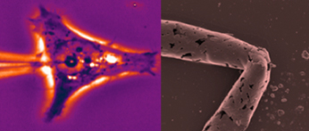 The Nano-Bio Interface Laboratory (NBIL) investigates several aspects critical to the interface of nanotechnology and biology, including nanomanufacturing, nanomanipulation, technology-biology interactions, and biomedical applications. The NBIL aims to create cutting-edge nanobiotechnology, advance knowledge in nanoscience and biology, and train the next generation of scientists and engineers at the interface of nanotechnology and biology. The NBIL is a diverse, multidisciplinary environment that fosters innovation to create practical nanobiotechnology for the betterment of society. Using a multidisciplinary approach to focus on multi-scale transport phenomena, biological functions and interactions, and mechanical and materials engineering, the NBIL studies micro/nanoscale fluid behavior and develops associated micro/nanotechnologies for biological metrology.
Alumni
Many graduates of the microsystems engineering doctorate program hold positions at semiconductor corporations—and the companies that use these complex, integrated circuit technologies—around the world. They are research scientists and materials research engineers on teams at the U.S. Naval Research Center; process integration engineers for Apple Inc., where they are developing next-generation display panels and sensors; directors of R&D at Megachips America Inc.; and research faculty at major universities. Companies that employ RIT’s microsystems engineering graduates include NASA, Intel, GE, Analog Devices, Samsung, IBM, Sandia National Laboratories, Texas Instruments, Global Foundries, Mentor Graphics, and the Interuniversity Microelectronic Center in Belgium.
Testimonials
 “While working toward my PhD in Microsystems at RIT, I was exposed to cutting edge technology with the opportunity to be part of industry supported research.” Anand is one of the earliest graduates from the Microsystems PhD program at RIT, doing his research in the area RF and analog mixed-signal technology. “I was part of a vibrant research environment and benefited from the multi-disciplinary nature of Microsystems – working in areas like semiconductor fabrication, device physics, and industrial engineering. My experience at RIT was immensely beneficial to the work I do now - leading diverse product teams to come up with real world engineering solutions.”
Anand is currently the VP of Engineering at Rambus Inc. where he leads the engineering organization towards the development of high speed memory and data link based products serving mobile, consumer and enterprise applications. Prior to joining Rambus, Anand worked at Megachips America Inc. where he was the Director of Research and Development, leading a global team to develop mixed-signal technology for several high volume ASICs.
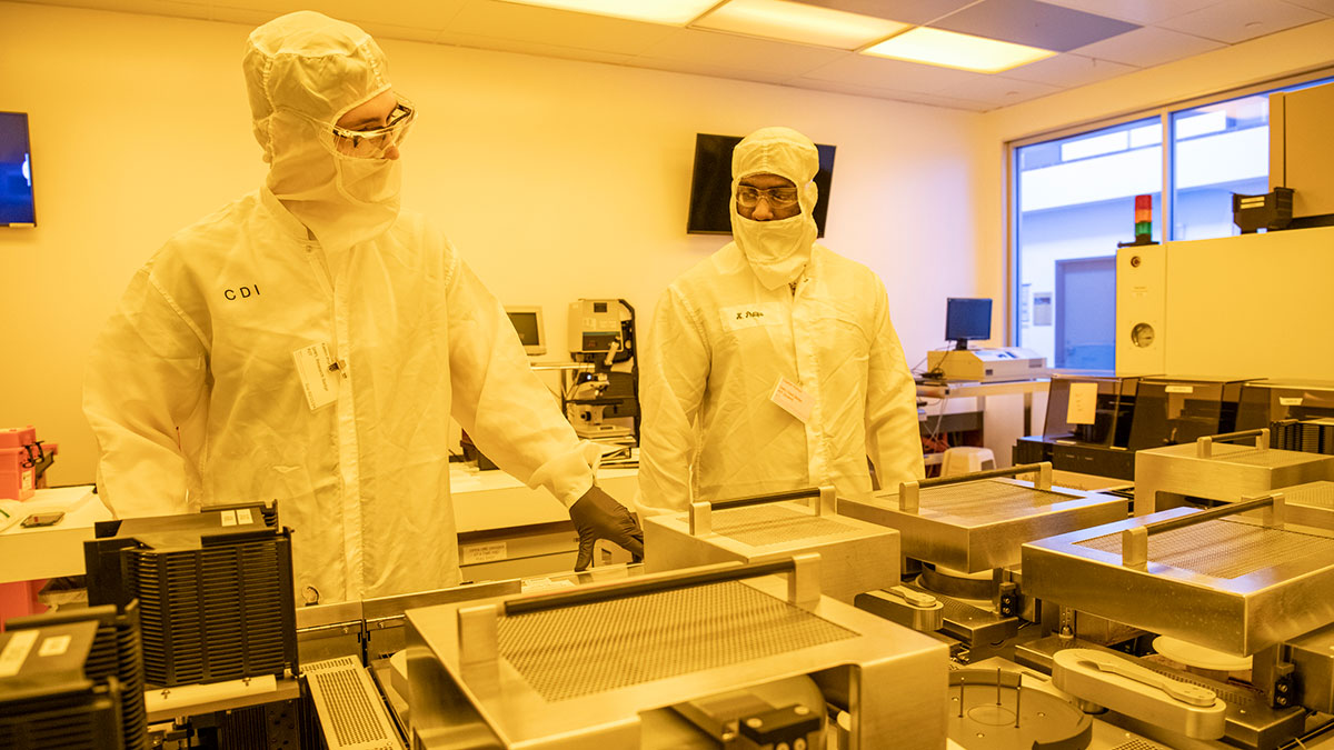
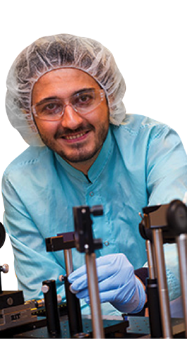 "I came from Turkey with good theory, and was able to put it into practice here. I had culture shock initially, but you get over it soon.” Coming to RIT meant changes in Burak’s life, but it also meant learning about the manufacturing process for integrated circuits, his initial reason for pursuing a degree at RIT.
“I had always heard there were limitations to design that is imposed by the manufacturing process, in the clean room, so I wanted to learn what was meant by that,” he says.
“I had access to the latest technology, tools and data,” says Baylav. “It was a dream come true and I was able to use this relationship for my Ph.D. research.”
One of Burak’s learning opportunities was a yearlong sponsored assignment through Mentor Graphics Corp. at the Interuniversity Microelectonics Centre (IMEC), a world-class semiconductor research facility located in Leuven, Belgium.
Burak now works in research and development in Resolution Enhancement Technology at Intel Corp. in Portland, Oregon
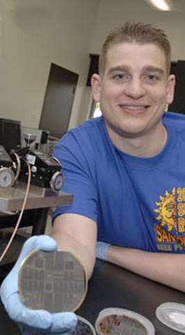 "During my time at RIT, I performed research in the NanoPower Research Labs. It was here that I learned how to create nanomaterials and devices. I learned how to understand them, and test their performance.
Now, I use these skills at the US Naval Research Lab in Washington, DC. My work here has a massive impact on how electronics are created.
Our research has allowed new processes and materials to be developed for harsh environments - like space. The research we do every day is on the cutting-edge.
The Microsystems Engineering Ph.D. program at RIT prepared me very well for this career. RIT's program gave me the experience that made my career possible."
Cory's Background
Dr. Cory Cress (RIT BS/MS – ‘03, Ph.D. – ‘08) is currently a Materials Research Engineer at the US Naval Research Laboratory in Washington, DC.
As a member of the Radiation Effects Section, Dr. Cress leads an effort studying the effects of radiation on bleeding-edge nanotechnology like:
- Si finFETs (L-channel = 14 nm)
- Integrated Ge/III-V finFETs
- Carbon nanotubes
- Graphene
- 2D-transition metal dichalcogenides (e.g., MoS2, WS2)
A primary objective of his work for the US government is to quantify how radiation affects device performance. This research will have impact for generations to come.
 Monica Kempsell Sears finds the biggest thrills in the smallest details of nanolithography and in manipulating wavelengths of light. But even she is surprised she found her focus so early.
“It’s so unusual to be so directed,” she says. “I feel lucky to be so passionate about something. A lot of people take a long time to figure out what their passion in life is. I fell in love with lithography in high school.” Monica finished her Ph.D. in Microsystems Engineering in 2013 and now works in the field of semiconductor lithography at Intel.
“I’ve always wanted to be one of the people who figures out how to push this field further and further—and now I am.”
 "I found my Microsystems experience prepared me well for the challenges of industry.
During my Ph.D. program, I had taken a 1-year internship at IMEC as well as a 4 months internship at GlobalFoundries.
These experiences helped me to better understand the workspace, expand my professional network and get a pulse of where the industry is heading.
With my solid preparation at RIT, I am confident that I am ready to take on any challenges in the future."
Peng's Background
Peng is currently a serion panel process engineer at Apple Inc.
At Apple, Peng is responsible for developing the next generation of display panels and sensors. In his previous positions, he worked at Applied Materials, a manufacturing company.
Peng is an award winning employee, has made contributions to various innovative products, and contributed to more than 10 patents.
Latest News
-
March 23, 2026
Awaiting green light as national hub
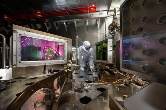
Rochester Beacon speaks to Stefan Preble, Bausch and Lomb Professor and Ph.D. program director of microsystems engineering, about the region’s bid to become a National Science Foundation innovation hub and how the STELLAR initiative could expand laser research and workforce development.
-
November 19, 2025

Manifesting quantum: How RIT researchers are navigating the next frontier of physics
RIT researchers are zeroing in on quantum photonics, the creation, control, and detection of light. Photonics has long been a specialty of the university. RIT led the team that developed the first quantum photonic wafer, which is key to the future of mass-produced quantum communication systems.
-
July 7, 2025

RIT, UR partner on first quantum communication experiment in upstate N.Y.
Spectrum News speaks to Stefan Preble, professor in the Kate Gleason College of Engineering, and microsystems engineering Ph.D. student Vijay Sundaram about the network.
Featured Profiles
RIT Alumnus Drives Innovation with Breakthrough Micro-LED Display Startup
Matthew Hartensveld, RIT alumnus and co-founder of Innovation Semiconductor, is pushing the boundaries of display technology with his pioneering work on micro-LED platforms.
Doctoral degree program
In RIT's microsystems engineering Ph.D., you’ll conduct research in nano-engineering, design methods, and technologies for micro- and nano-scaled systems.
Learn more about the Microsystems Engineering Ph.D. programStudent Resources
The Microsystems Engineering Ph.D. offers a variety of resources for our students that range from academic support to handbooks and more. Visit our Student Resources for more information.


